Thesis
In February 2024, Sam Altman posted on X that OpenAI was generating about 100 billion words per day. A year later, Google announced in April 2025 that it was processing 480 trillion tokens per month (or roughly 12 trillion words a day). To sustain these growth levels, more compute is needed. Consequently, OpenAI announced in January 2025 that it was building a 5GW AI datacenter for $500 billion. Not to be outdone, in July 2025, Mark Zuckerberg announced that Meta would also build Hyperion, a 5GW AI datacenter, exceeding an earlier 1GW AI datacenter deployment by Meta called Prometheus in Ohio.
Yet, despite all the hype around Nvidia, GPUs, and other AI accelerators, it is interesting to note that compute is no longer the bottleneck for AI progress. As the AI infrastructure buildout race has revealed, compute capabilities are continuing to scale thanks to Nvidia, as well as other notable AI accelerator startups like Cerebras and Groq, but data movement and bandwidth have not scaled as fast. It has been well-established that the rate of memory bandwidth improvements has increased more slowly than raw compute (in FLOPs) for years. Known as the memory wall problem, LLMs are now bottlenecked by how fast data can transfer between the computation and memory unit of a chip. The maximum rate at which this data transfer can occur is the chip’s memory bandwidth.

Source: Ayar Labs
In a simplified sense, LLMs mathematically depend on massively parallelized matrix multiplications (MatMuls) to operate. However, during MatMul operations, a GPU (or other type of AI accelerator) must read both matrices from memory, perform the computation, then save the result back to memory — and because intra-GPU data movement is not instantaneous (limited by the speed of signal propagation), this takes a certain, non-zero amount of time.
Furthermore, because SOTA models have billions or even trillions of parameters, a model must be “cut up” and spread across multiple GPUs. Consider the open-source LLaMa 3-70B model (a medium-sized model) running on a typical Nvidia H100 GPU, which has 80GB of on-chip memory. Just to load the model onto the chip requires roughly 70GB of memory (at quantized INT8 weights; using FP16 weights alone requires roughly 140GB). Note that this doesn’t include additional overhead from the KV-cache or user-inputted prompt tokens! Thus, even this medium-sized model needs to be sharded across multiple H100 GPUs via tensor or pipeline parallelism. Thus, inter-GPU data movement is required to share the partial MatMul results between multiple GPUs so that they can work in synchrony.
All of this results in GPUs being idle while waiting for data transfers at training and inference time. Several papers have found that large-batch inference results in 50% of GPU cycles remaining idle due to data-fetch delays. Communication overhead has dominated the runtime of these models, where terabytes of data need to be exchanged for a single forward-pass step during inference. If LLMs continue to get larger, one must surpass the current memory wall.
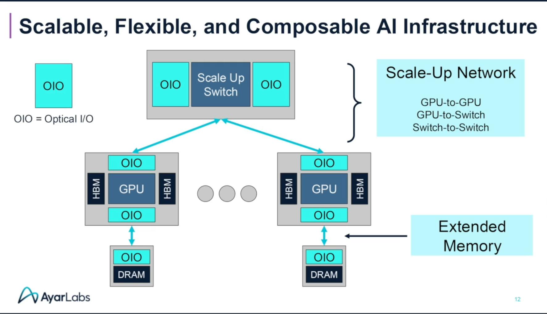
Ayar Labs is a silicon photonics-based interconnects company that replaces electrical interconnects with high-speed, light-based links between chips. The company’s flagship product, TeraPHY, is an optical chiplet that allows other chips to transfer 8 Tbps of bandwidth at extremely low latencies (10 nanoseconds) and superior power efficiency compared to current conventional solutions. With this solution, Ayar Labs aims to eliminate the intra-GPU and inter-GPU communication bottlenecks that currently plague distributed AI systems and offer a solution to surmount the memory wall problem.
Founding Story

Source: MIT News
Ayar Labs was founded in 2015 by Mark Wade (former Chief Scientist, CEO), Alex Wright-Gladstein (former CEO, Advisor), Vladimir Stojanovic (former Chief Architect, CTO), and Chen Sun (former CTO, Chief Scientist). The company was also supported and co-founded by Rajeev Ram, head of Physical Optics and Electronics Group at MIT, and Milos Popovic, former assistant professor at CU Boulder’s Optical Devices Lab.
Stojanovic was an associate professor of electrical engineering and computer science (EECS) at MIT before transferring to Berkeley as an adjunct professor of EECS. With expertise in VLSI semiconductor design and high-speed linkage, Stojanovic previously co-founded NanoSemi in 2014, which was later acquired by MaxLinear for roughly $96.8 million in September 2020.
Meanwhile, Ram headed the Physical Optics and Electronics group at MIT, where he was recruited by DARPA alongside Stojanovic. Initially skeptical of photonics, the use of existing electronic material in his lab to create optical devices — waveguides, wavelength filters, modulators, and detectors — packing them on a microchip provided him with belief in the field.
Ayar’s core technology began with a research collaboration in the mid-2010s at MIT as part of DARPA’s Photonically Optimized Embedded Microprocessors (POEM) project. The project was a joint collaboration between Berkeley, MIT, and CU Boulder, led by Stojanovic, in collaboration with Ram and Popovic. The collaboration resulted in a 2015 paper in Nature, showcasing a three-by-six millimeter, light-enabled microprocessor combining 70 million transistors and 850 photonic input/output (I/O) components. This led Stojanovic, Ram, and Popovic to realize that a low-power, yet high-performance photonic computing chip was possible. The chip was shown in lab to have a bandwidth of 300 gigabits per second per square meter, which was about 10-50 times greater than existing electrical microprocessors at the time. Wade and Sun were both working on the project as graduate researchers and were the main co-authors behind the 2015 paper.
Wade started his scientific career at Louisiana Tech, where his childhood fascination with astronomy and the cosmos led him to study physics and electrical engineering. While visiting graduate schools, he discovered silicon photonics and pursued a PhD in the field at the University of Colorado, Boulder. After receiving his PhD, where he built the first-ever CPU-to-memory photonic interconnect, Wade sought to continue his research in photonics at MIT. There, he was part of a breakthrough that implemented optical technology to be built into existing silicon chip design to replace copper wires, which improved efficiency through reduced heat waste. Sun was a PhD candidate in EECS at MIT, and was working as a graduate research assistant in the photonics field as part of Stojanovic’s lab. Sun had also previously interned at Rambus, a semiconductor company, and Nvidia.
Prior to founding Ayar Labs, Wright-Gladstein was an MBA student at MIT and had previously pursued a bachelor's in economics and political science at Tufts University. Before pursuing her MBA, she worked at a cleantech startup called EnerNoc, before deciding that she wanted to meet more people working on climate-based technologies. At MIT, Wright-Gladstein met Wade and Sun while TAing for a class called Energy Ventures. For the class, she handpicked a dozen out of the 300 labs at MIT that pursued energy-related research, and prompted them to compete at MIT’s clean energy competition. The team that eventually won was known as OptiBits, which received $275K at the competition, comprising the $75K Department of Energy Clean Energy Prize and the $200K Eversource Clean Energy Grand Prize. This team eventually became the start of Ayar Labs.
Ayar Labs later added Charles Wuischpard as CEO of the company in 2018, who previously was the CEO of Penguin Computing and held previous roles at Intel. In 2023, he left Ayar Labs to join Nvidia as Vice President of Americas. Lisa Cummins Dulchinos joined as CFO in 2019 with previous roles at Penguin Computing and Adept Technology. Her experience includes managing M&A, securing financing, and leading Sarbanes-Oxley (SOX) compliance, with experience in financial leadership for a capital-intensive hardware startup.
Amelia Thornton joined Ayar Labs as Chief People Officer in December 2021, previously serving as president of The Thornton Group, a global consulting firm. In January 2024, Ayar Labs announced the additions of Ganesh Moorthy and Craig Barratt to the Board of Directors. Moorthy was the former President and CEO of Microchip Technologies and has had several senior leadership roles at Intel. Barratt was the former CEO of Atheros and has held executive positions at Google, Qualcomm, and Intel. In October 2025, Vivek Gupta, who was previously the Head of Telco industry at Google Cloud and prior to that a VP at Qualcomm, joined Ayar Labs as the company’s first Chief Strategy Officer.
Product
Source: Ayar Labs
Ayar Labs’ goal is to solve the problem of data transfer bottlenecks caused by shortcomings of traditional interconnects. The increasing complexity and size of LLM AI models are starting to overwhelm current data center infrastructure based on traditional interconnect technologies. Whereas compute was scaling with newer silicon chips, data movement in and out of the chip was becoming increasingly difficult. With Ayar Labs’ approach of transmitting data through light-based processing, they hope to continue to scale computing system performance.
Why Photonics?
Source: Ayar Labs
Photonics, the use of light for transmitting information, possesses several properties much more advantageous compared to the electron. While photonics developments have been widespread in the field of telecommunication through optical fiber cables, it was not until the 21st century that photonics was being implemented for computing.
Traditional copper wires are susceptible to "crosstalk" and electromagnetic interference (EMI), where the signal from one wire corrupts the signal in an adjacent one. This physical limitation puts a hard cap on how much data can be densely packed and transmitted. To solve this, copper-based solutions added retimers to be placed periodically along the channel to recover the lost data signal, which increases cost and latency.
Additional problems of traditional copper interconnects stem from their signal degradation. Over distances of more than a few centimeters, high-frequency electrical signals degrade rapidly, requiring costly and power-hungry repeater or amplifier chips to boost the signal. Currently, copper-based solutions limit the range of connectivity between chips to a few inches in PCBs to a few meters in copper cables. The insertion loss of copper-based interconnects scales inversely, meaning every generation of copper connectivity has to sacrifice some distance for improved signal bandwidths. Additional costs stem from the use of more expensive packages and PCBs (either higher quality manufacturing or with more layers), which are needed to maintain signal integrity. As data centers and computing clusters continue to scale in size, communication between chips, memory, storage, and network will transmit over longer and longer distances, making copper interconnects unsuitable for the task at hand.
Finally, electrical resistance turns a significant portion of energy into waste heat. As data rates climb into the gigabits per second, the power required to drive a clear signal across even short distances on a circuit board becomes unsustainable, contributing massively to the enormous energy footprint of data centers.
By switching to a photonics-based approach of using light to transmit information, some inherent properties may allow for the aforementioned problems to be solved. One crucial property of photonics is its ability to parallel process and handle massive amounts of data. Since different wavelengths of light can be transported simultaneously, higher bandwidth communication is made possible, allowing for various data streams to run and be processed simultaneously. Additionally, reduced latency can be achieved, as light travels faster than the drift velocity of electrons in copper wires. Still, the rate at which an optical transistor can respond to a signal is limited by its spectral bandwidth, making these advances limited.
In terms of distance, optical signals suffer significantly less attenuation over long-haul transmissions when compared to electronic waveforms. This property helps provide accurate and reliable communication among different elements in a data center, and may also be applicable to quantum computing. Energy efficiency is also a significant advantage. Photonics can lead to reduced heat generation, which translates to less complex cooling systems and lower power requirements compared to conventional electronic circuits. However, it's worth noting that this benefit may be offset by the energy consumption during manufacturing.
While still largely in the research and development phase, other promising applications of photonics not yet applicable in the near future include quantum computing with optics, optical neural networks for machine learning, optical quantum key distribution, and optical signal and image processing.
Product Offerings
Source: Ayar Labs
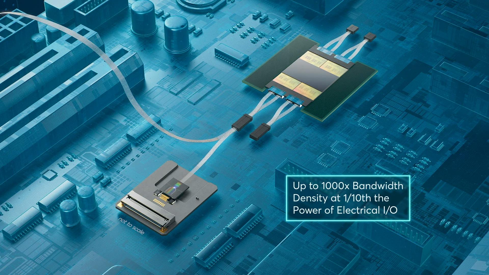
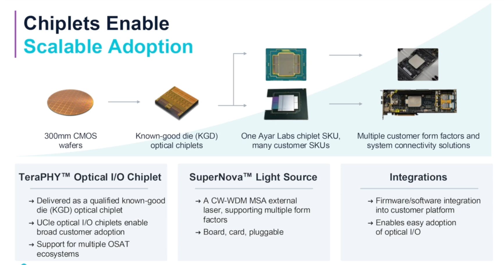
The TeraPHY is Ayar Labs’s core offering. It is a monolithic silicon chiplet that serves as a bridge between the electrical domain of a host processor and the optical domain of the fiber network. Designed to be co-packaged directly next to a GPU or CPU, it functions as a high-bandwidth interconnect alternative to traditional copper backplanes and pluggable optics. As Matt Thorn, Ayar Labs’ VP of Commercial Operations, explains, “Our TeraPHY family of in-package optical chiplets can be packaged with a compute chip to convert data traffic on light into data traffic with electrons... It allows TeraPHY to talk to the system on chip (SOC) in the language it understands, which is electrons, while talking between packages with photons.”
While most optical chips use large Mach-Zehnder modulators to encode data, which limits the ability to pack many channels densely, Ayar Labs utilizes micro-ring modulators. Although notoriously difficult to manufacture reliably, these modulators are far smaller and more efficient. This allows Ayar Labs to use significantly less silicon than equivalent pluggable optical transceivers and consume up to 3x less power per bit transferred. The TeraPHY is manufactured using an industry-standard Global Foundries 45nm platform, integrating both electrical and photonic circuits onto a single die. The second generation, released in 2025, moved to the industry-standard Universal Chiplet Interconnect Express (UCIe) package, ensuring it can fit into existing system-in-package architectures. Optimized for the demanding workloads of AI, each TeraPHY port can carry up to 16 channels of light, equivalent to an x8 PCIe Gen6 link.
Source: Ayar Labs
Completing the optical I/O solution is the SuperNova, an external light source. Functioning much like a power supply for the optical system, the SuperNova is a distributed feedback (DFB) laser array that provides up to 16 wavelengths of light, capable of powering up to 16 TeraPHY ports. It is the first optical source designed to be compliant with the CW-WDM MSA (Continuous-Wave Wavelength Division Multiplexing Multi-Source Agreement) specifications, enabling a total of 256 data channels for a bidirectional bandwidth of 16 Tbps. Together, they hope to eliminate communication lags between multiple GPUs, just in time for the next generation of LLMs that require entire clusters.
Market
Customer
Ayar Labs targets a broad spectrum of customers across multiple compute-intensive verticals, focusing on those pushing the boundaries of data movement and processing. Their primary customers are leading semiconductor manufacturers, hyperscale cloud providers, AI infrastructure companies, and system integrators who are building the next generation of data centers, AI clusters, and high-performance computing (HPC) systems. Major industry players such as NVIDIA, Intel, AMD, Hewlett Packard Enterprise, and Fujitsu are actively investing or integrating Ayar Labs’ optical I/O technology in their current computing infrastructure.
Beyond the core tech giants, Ayar Labs' customer base extends to large enterprises in sectors like financial services, life sciences, and energy that require massive compute and data movement capabilities for their advanced AI and HPC needs. Executives from Google, OpenAI, and Lawrence Livermore National Lab have been featured on their website, citing the importance of next-generation interconnects.
The technology also finds critical applications in specialized industries. In aerospace and defense, companies like Lockheed Martin and Raytheon are piloting the technology for advanced radar, phased array, and sensor fusion platforms, where high bandwidth, low latency, and resistance to electromagnetic interference (EMI) are essential. Similarly, in the telecommunications sector, partners such as Ericsson and Corning are working with Ayar Labs to enable next-generation 5G/6G radio and edge infrastructure. Finally, other semiconductor companies, such as Advanced Semiconductor Engineering (ASE), Alphawave Semi, and d-Matrix, develop products that work in parallel with Ayar Labs’ interconnects.
Market Size
The market opportunity for Ayar Labs is driven by the rise in AI, HPC, and data center infrastructure, all of which are facing critical bottlenecks due to data movement and interconnect bandwidth. AI and data center infrastructure spending is expected to exceed $1 trillion from 2025-2035, with optical I/O and chiplet-based architectures seen as foundational technologies for scaling compute and memory.
The broader market trends are highly favorable. The global optical interconnect market, which includes more traditional technologies like those for telecom, is estimated at $16.1 billion in 2024 and is projected to reach $34.5 billion by 2030, growing at a CAGR of 14.1%. The more specific silicon photonics market, where Ayar Labs operates, shows even more dramatic growth potential. While one estimate valued it at $95 million in 2023 with a projection to reach over $863 million by 2029, with other analyses projecting the market to reach as high as $9.7 billion by 2030, reflecting a much higher CAGR of 29.5%. Ayar Labs' specific target sector, UCIe optical chiplets, was valued at approximately $35 million in 2024 and is projected to grow to $520 million by 2030.
Looking ahead, Ayar Labs' CEO Mark Wade predicts the market for on-chip optical I/O will begin to mature between 2026 and 2028, followed by a "proliferation across a broad industry base" beyond that timeframe. The company itself estimates that by the end of the 2020s, the photonics IC market could exceed $38 billion, with annual chiplet shipments surpassing 100 million units.
Competition
The market for next-generation photonics hardware is being contested on two primary fronts: specialized startups focused on optical computing, and established semiconductor incumbents who are strategically integrating optical technologies to defend and improve their market positions.
Startups
Lightmatter: Lightmatter offers both photonic interconnects (Passage) and a full AI accelerator (Envise), which can run neural network computations by itself. Compared to Ayar Lab’s TeraPHY chiplet and SuperNova light source, Passage prioritizes edgeless I/O across the entire die area, compared to the more modular approach of Ayar Labs. In April 2025, the company released the latest iteration of the Passage, the L200 and L200x, which claims over 200 Tbps of total I/O bandwidth, resulting in 8x faster training times for advanced AI models. Valued at $4.4 billion, Lightmatter has raised $822 million as of October 2025.
Celestial AI: Celestial AI specializes in high-performance memory and interconnect solutions using silicon photonics technology. Its main offering is the Photonic Fabric, an interconnect technology offered through a chiplet, switch, or packaging form. Compared to Ayar Labs, its offerings are attempting to be more “full stack”, with products for the entire server rack. As of October 2025, the company has raised $593.9 million, including a $250 million Series C1 in March 2025, and employs 137 people.
Neurophos: Neurophos, founded in 2020, is advancing complete photonic computing units (OPUs) to replace traditional electronic processors entirely. While specific updates in mid-2025 are limited, the company is positioned as a challenger in optical computing paradigms, aiming for energy-efficient alternatives to silicon accelerators in AI and high-performance computing (HPC) workloads. Neurophos raised $7.2 million in its 2024 seed round, led by Gates Frontier and supported by MetaVC and Mana Ventures.
nEye Systems: Originating from UC Berkeley in 2020, nEye Systems is developing wafer-scale optical circuit switches for dynamic, high-speed data routing in AI data centers. In April 2025, it raised $58 million in Series B funding led by CapitalG (Alphabet's growth fund), with participation from Microsoft's M12, Micron Ventures, Nvidia, and Socratic Partners, bringing total funding to over $72 million. Prototypes are said to be complete, with production samples expected in 2026. The technology promises 100x smaller size, 1,000x energy efficiency, and 10,000x speed over electrical switches, with intelligent reconfiguration for optimal chip-to-chip connections.
Incumbents
Established semiconductor giants are integrating photonics to enhance their AI and HPC offerings, leveraging their scale for rapid adoption and integration.
AMD: AMD is advancing integrated photonics via its acquisition of startup Enosemi, focusing on optical I/O for future CPUs and GPUs. AMD hopes to integrate Enosemi’s talent to develop a variety of photonics and co-packaged optics solutions for next-generation AI systems. Before the acquisition, Enosemi offered chiplets with photodetectors, optical IPs, and custom silicon services.
Nvidia: Nvidia leads the AI chip market and has expanded into photonics with its Spectrum-X and Quantum-X platforms, incorporating co-packaged optics for GPU interconnects. Expected to be available in late 2025, the Quantum-X is a photonic switch that provides 144 ports of InfiniBand and utilizes a liquid-cooled design. The Spectrum-X consists of both an Ethernet Networking platform and photonic switches, which can be configured to 128, 512, or 2048 port configurations, and is expected to be available in 2026.
TSMC: TSMC, as the leading foundry, has signed multiple partnerships working on integrated photonics capabilities. Ansys is collaborating with TSMC on the Compact Universal Photonics Engines (COUPE), which is a co-packaged system optics platform aiming to mitigate coupling loss while accelerating chip-to-chip and machine-to-machine communication. Strategic partnerships with Cadence and Synopsys have also been developed, with photonics being one of the targeted areas.
Corning: Corning is developing co-packaged optics infrastructure in collaboration with Broadcom, focusing on glass substrates and packaging to boost data center processing capacity. Broadcom and Corning showcased co-packaged optics implementations, including the Tomahawk Ultra switch for scale-up networks, showcasing Corning's role in enabling dense optical-silicon integration.
Business Model
Ayar Lab’s primary business model is to license and sell its optical I/O solutions directly to semiconductor manufacturers, hyperscale data center operations, and system integrators. The company’s core products, the TeraPHY optical chiplet and SuperNova light source, are sold as a co-packaged offering designed for integration into next-generation CPUs, GPUs, and AI accelerators. While its pricing remains unavailable to the public, Ayar Labs has demonstrated some early commercial traction, shipping approximately 15K units to select customers as of December 2024.
The company projects aggressive growth, forecasting annual shipments to exceed 100 million units by 2028. As a pure-play optical provider, Ayar Labs is also exploring alternative revenue streams, including licensing its technology to Tier 2 and Tier 3 vendors like fabless companies focusing on RISC-V, though they stated that this would not be an immediate focus. Additional income is generated through strategic collaborations, such as agreements with Hewlett Packard Enterprise and Lockheed Martin, to integrate silicon photonics into their respective infrastructures.
Traction
Ayar Labs has made consistent progress in advancing optical interconnect technology, leveraging silicon photonics to address the growing demands of modern computing. In 2017, the company introduced its first prototype, a 45nm optical chip built on a commercially available CMOS process, and entered into a strategic collaboration with GlobalFoundries to scale its innovations. The following year, Ayar Labs showcased a photonics chiplet integrated into evaluation boards with Intel FPGAs, demonstrating its potential for high-performance computing applications.
In 2019, Ayar Labs was selected as the optical solution provider for Intel’s DARPA PIPES project, further cementing its role in cutting-edge optical interconnect development. By 2020, the company had achieved a significant milestone by demonstrating an ultra-dense optical interconnect solution on GlobalFoundries’ silicon photonics manufacturing process. That same year, Ayar Labs joined the CW-WDM MSA group to help establish industry standards for multi-wavelength optical laser sources, aligning with its SuperNova laser technology.
The momentum continued in 2021 with a partnership with MACOM, which enabled the demonstration of the first terabit optical link for co-packaged optics and chip-to-chip connectivity. By 2022, Ayar Labs transitioned into its commercialization phase, delivering its first volume shipments. In 2023, the company expanded its partnership with Sivers Photonics, placing a $1 million order for light source technology to support the growing demand for generative AI infrastructure. In 2024, Ayar Labs began shipping thousands of engineering samples of its optical chiplets, allowing manufacturers to refine their production, testing, and packaging processes in preparation for large-scale deployment.
In July 2025, Ayar Labs announced the opening of a new office in Taiwan and doubled the size of its San Jose headquarters. In September 2025, Ayar Labs announced a partnership with both Taiwanese ASIC packaging company AIchip and TSMC, with the goal of accelerating the production of the company’s optical chiplets.
Valuation
Ayar Labs has steadily grown its financial backing, securing funding across multiple rounds from venture capital firms and computing companies alike. In November 2020, the company closed its Series B funding round, raising $35 million. The round was co-led by Downing Ventures and BlueSky Capital, with new investors such as Applied Ventures, Castor Ventures, SGInnovate, and Downing Ventures joining existing backers like Intel Capital, Lockheed Martin Ventures, Global Foundries, and Playground Global.
In April 2022, Ayar Labs raised $130 million in Series C funding, bringing Hewlett Packard Enterprise (HPE) and NVIDIA on board as investors.
By December 2024, Ayar Labs had raised $155 million in Series D funding, led by Advent Global Opportunities and Light Street Capital. Major industry players like AMD Ventures, Intel Capital, NVIDIA, and 3M Ventures also participated. This round brought Ayar Labs’ total funding to approximately $372 million and pushed its valuation to over $1 billion. The funding positions Ayar Labs among private AI hardware peers such as Groq ($2.8 billion), SambaNova ($5 billion), Tenstorrent ($2.7 billion), Cerebras ($4 billion), and Lightmatter ($4.4 billion).
Key Opportunities
Need for High Bandwidth Interconnects for AI/ML Workloads
The increasing computational demands of AI and machine learning workloads present a significant opportunity for Ayar Labs. NVIDIA CEO Jensen Huang has stated that next-generation AI models will require 100 times more compute than current models due to advancements in reasoning approaches. By 2030, data centers are projected to require nearly $7 trillion in capital outlays, highlighting the need for scalable, high-performance infrastructure.
Ayar Labs’s optical I/O technology addresses the limitations of copper-based systems, enhancing link density and enabling nodes to function as a single unified GPU, which is critical for scaling AI workloads. Bill Dally, Chief Scientist at NVIDIA, emphasized Ayar Labs’s importance: “Optical connectivity will be important to scale accelerated computing clusters to meet the fast-growing demands of AI and HPC workloads. Ayar Labs has unique optical I/O technology that meets the needs of scaling next-generation silicon photonics-based architectures for AI.”
Thermal Efficiency and Power Savings
As data centers are projected to consume 8% of total US electricity by 2030, energy efficiency has become a critical concern. With renewable energy sources like solar and wind expected to meet only 40% of this demand, reducing power consumption is essential. Ayar Labs’ optical interconnects offer potential thermal and energy efficiency advantages over traditional copper-based systems, aligning with the net-zero goals of major tech companies.
Strong Industry Support
Ayar Labs benefits from significant investments and partnerships with industry leaders such as NVIDIA, Intel, AMD, and GlobalFoundries. These collaborations not only provide capital but also facilitate the integration of Ayar Labs’ technology into mainstream platforms. Additionally, partnerships with manufacturing leaders like GlobalFoundries, TSMC, Sivers Photonics, and Lumentum position the company to scale production effectively.
Applications Beyond AI and Data Centers
Ayar Labs is exploring applications in telecom, aerospace, and defense. For example, partnerships with Lockheed Martin and Ericsson are investigating how optical I/O can improve radar and telecom systems by reducing weight and increasing data rates. Lockheed Martin’s CTO, Steve Walker, highlighted Ayar Labs’s role in the future of defense. “As the complexity and amount of data grows on the battlefield, faster decision-making is essential. New innovative system architectures, coupled with AI and machine learning techniques, are needed for our customers’ mission success. Ayar Labs’ optical interconnect solution provides the necessary technology to process spectral information with greater speed and lower latency for next-generation system designs.” Additionally, Ayar Labs is working on digital beamforming solutions using optical transport mechanisms, which could improve radar and phased array systems.
Key Risks
Manufacturing and Supply Chain Complexity
Optical I/O manufacturing is less mature and more complex than traditional semiconductor production, requiring specialized photonics manufacturing, integration, and testing. The company relies heavily on GlobalFoundries for device manufacturing, which could become a bottleneck given the high demand for silicon photonics capabilities from other companies like Broadcom, Marvell, Lightmatter, PsiQuantum, Ranovus, Xanadu, Ansys, Cadence, Synopsys, and NVIDIA. Additionally, trade and tariff issues could further complicate the supply chain, as many components are sourced internationally, adding another layer of risk to production scalability.
High Cost of Integration with Existing Infrastructure
The UCIe interconnect standard, established in 2022, is still in its early stages, meaning most existing chips are not yet compatible with Ayar Labs’ optical I/O. While UCIe has a clear scaling roadmap, integrating optical components with current electronic systems remains a complex and costly process. Connecting processors requires specific interfaces, and the reliability of optical systems over long ranges can be a concern, further complicating adoption.
Reliability and Environmental Sensitivity
Reliability and environmental sensitivity are additional risks for Ayar Labs. Optical systems are highly sensitive to environmental factors such as temperature and humidity, which can impact their performance and increase costs. Current solutions, such as sealing components in hermetic packages or using protective coatings, add complexity and expense to the manufacturing process. Signal fading and integration issues in optical systems can also affect reliability, particularly in large-scale deployments, posing a challenge for widespread adoption.
Lack of Standardized Testing Infrastructure
The lack of standardized testing infrastructure further complicates Ayar Labs’s ability to scale. Testing optical devices is a multi-stage, resource-intensive process. Wafer-level testing requires micrometer-level precision in fiber alignment, and photonic integrated circuits must be tested again before integration into co-packaged devices. The lack of automation in testing processes further complicates scaling, and existing systems may not support the specific connectors required for optical I/O. These challenges make it difficult to streamline production and ensure consistent quality at scale.
Intense Competition
Finally, Ayar Labs faces intense competition in the photonics market. Companies like Lightmatter and Celestial AI are developing similar technologies, and Ayar Labs must differentiate itself to maintain its position. Additionally, incumbent chipmakers like NVIDIA and AMD are also working on photonics technology, which may be more easily integrated with their existing products. While Ayar Labs’ technology offers unique advantages, the competitive landscape remains a significant hurdle to its long-term success.
Summary
Ayar Labs sits at the heart of a massive investment influx in data center technology, where its optical I/O technology is poised to become an important piece for the next generation of AI, cloud, and high-performance computing infrastructure. By enabling ultra-high bandwidth, low-latency, and energy-efficient data movement between chips, Ayar Labs offers a solution to the data bottlenecks that limit today’s largest AI and HPC systems. Its deep integration with industry giants, such as AMD, Intel, NVIDIA, TSMC, and HPE, positions Ayar Labs as a critical enabler for the world’s leading semiconductor and cloud companies.
Unlike traditional interconnect providers, Ayar Labs leverages a standards-driven, ecosystem-first approach, championing open chiplet standards (like UCIe) and collaborating with a broad network of foundries, photonics suppliers, and system integrators. This strategy not only accelerates adoption but also ensures interoperability and scalability across the industry. As AI models and data centers scale exponentially, Ayar Labs’ optical I/O is uniquely suited to meet the surging demand for bandwidth and efficiency, opening up new markets in telecom, aerospace, defense, and beyond. However, Ayar Labs’ long-term success will depend on its ability to move from pilot deployments to mass adoption, outpace well-funded competitors, and prove the reliability of its technology at hyperscale.