

Thesis
Global energy demand for data centers is expected to double by 2026, reaching levels equivalent to Japan's total electricity consumption. As of October 2024, data centers specialized for AI workloads drive 70% of this increased energy demand. This comes as a result of the energy-intensive nature of training foundational AI models and the continuous inferencing of AI models through services such as OpenAI’s ChatGPT or Anthropic’s Claude platforms.
For example, ChatGPT, with 200 million active weekly users as of August 2024, consumed approximately 564K kilowatt-hours of energy per day. Six months later, ChatGPT’s weekly users had doubled to 400 million, indicating that its energy use had likely doubled, indicating a rapid rate of growth in AI energy demand. Even Deepseek, which became known for developing an R1 model that reportedly was more efficient than competitors, may be equally or more energy-intensive to run.
Another factor leading to increasing energy consumption by data centers is the growing energy cost of cooling them. Traditional cooling systems struggle to manage the heat generated by AI processors, with cooling components requiring constant power to prevent overheating. In response, new methods such as liquid cooling are being tested to increase data center cooling efficiencies. As of August 2024, 22% of data centers used liquid cooling methods, with adoption projected to reach 50% by 2029.
Lightmatter is a company that develops specialized chips and chip communication technology, called interconnects, using photonics. By leveraging light for data processing and communication, Lightmatter aims to improve computational power while reducing energy consumption, particularly for AI workloads and data-intensive applications. Lightmatter’s CEO, Nicholas Harris, has stated that “over the next few years, all of the GPUs in the world that are designed for AI training and inference… are going to be built on Lightmatter’s Passage”, its photonic interconnect product to improve data center scale-out while reducing energy requirements otherwise impossible with conventional interconnect technologies.
Founding Story

Source: CNBC
Lightmatter was founded by Nicholas Harris (CEO), Darius Bunandar (Chief Scientist), and Thomas Graham (former COO & CFO) in September 2017.
Prior to founding Lightmatter, Harris worked as an R&D engineer at Micron Technologies in 2005, working on DRAM and NAND circuits and device physics. During his time at Micron, Harris studied integrated chips and realized that limitations in traditional computing advancement would slow down advancements in computing. To “figure out how he could continue [the roadmap for computing]”, Harris left Micron and completed his PhD and postdoctorate in electrical engineering and computer science at MIT.
During his time at MIT, Harris began exploring quantum computing technologies and once again identified gaps in the field. His doctoral thesis, "Programmable Nanophotonics for Quantum Information Processing and Artificial Intelligence," explored a potential solution through nanophotonic architectures. He also led MIT's quantum photonics lab, where he built silicon-based integrated photonic chips that processed information using light instead of electricity. As a researcher, Harris authored 69 academic articles and 17 patents.
His research and interest in photonics led to the initial concept for Lightmatter. Harris noticed that ”everybody knew that deep learning was going to be a huge deal”, so he “started learning more about it, and realized that the systems [he] was building for photonic quantum computing could be leveraged to do deep learning.” This realization prompted Harris to abandon his plans to become a professor following his PhD. Instead, he co-founded Lightmatter with Bundahar, another member of his photonics lab, and Graham, another student at MIT’s MBA program in 2017. That same year, the new startup won $100K through the MIT Entrepreneurship Competition.
Prior to Lightmatter, Bunandar earned degrees in physics and mechanical engineering from UT Austin in 2013, followed by a PhD in physics from MIT in 2018, completing his doctorate one year after founding Lightmatter. Graham, meanwhile, worked in various finance, operations, and business development roles at Morgan Stanley and Google. Graham completed his MBA from MIT's Sloan School of Management in 2018, also one year after founding Lightmatter.
Since 2017, Lightmatter has experienced several leadership changes. Graham served as Chief Operating Officer (COO) until May 2023, when he transitioned to Chief Financial Officer (CFO). In July 2024, Simona Jankowski (CFO) replaced Graham, bringing experience as managing director at Goldman Sachs and vice president of investor relations & strategic finance at NVIDIA. As of February 2025, Graham maintains a full-time position at Lightmatter with his job title being “founder”.
Product
For several decades, computing power advanced according to two key trends: Moore's Law, which observed that transistor counts on circuits would double every two years, and Dennard scaling, which states that as transistors shrink, their power density remains constant. These trends made computing cheaper, faster, smaller, and more energy efficient. However, these improvements began to slow around 2005.
Noticing the limitations of traditional chips, Lightmatter’s CEO and founder Harris believed that photonics chips would be a solution to continue these scaling observations. According to Harris,
“With photonics, you can perform multiple calculations at the same time because the data is coming in on different colors of light. In one color, you could have a photo of a dog. In another color, you could have a photo of a cat. In another color, maybe a tree, and you could have all three of those operations going through the same optical computing unit, this matrix accelerator, at the same time. That drives up operations per area, and it reuses the hardware that's there, driving up energy efficiency.”
The company created two main products to address different aspects of computing limitations. Passage, an optical interconnect chip, enables ultra-high data rates between memory cores and servers to accelerate data communication within data centers. Envise, a photonic computing chip, executes deep learning computations using tiny optical components to reduce power consumption and increase processing speeds.
Passage
Source: Lightmatter; Contrary Research
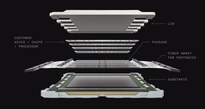
Lightmatter's Passage is a silicon photonics interconnect system that uses light, instead of electrical signals, to transmit data between computing components. In doing so, Lightmatter’s approach addresses the primary bottleneck in AI training and inference: limited scalability due to data movement constraints.
In computing clusters with many GPUs, the main bottleneck is in data movement. Most of the energy, and thus electrical costs, in computing is not spent on the matrix multiplication operations in AI models, but in reading and writing from memory to compute cores. Although existing fiber-optic technology has existed to facilitate enormous data movement at high speeds, this is typically done between long distances, such as across oceans for intercontinental connections. Lightmatter’s Passage miniaturizes this fiber-optic technology through silicon photonics on a single-chip scale.
Technically known as an interposer, Passage acts as a bridge between components to be connected and communicate with each other. For example, Passage can be sandwiched between two computing components, such as a processor and SRAM memory, allowing data to optically move between Passage. This interconnect system therefore supports high-speed bandwidth in chip-to-chip and node-to-node communication through Lightmatter’s optical I/O technology.
Passage also integrates with existing off-the-shelf chips, enabling companies to adopt Lightmatter’s interconnect technology without overhauling existing infrastructure. Passage delivers optical switching speeds of 100 Tbps for photonic, CPU, or GPU processing applications. It also supports up to 48 individual photonic, CPU, or GPU chips mounted directly on the interconnect. Passage’s design includes 40 photonic lanes, which together occupy the width of a single optical fiber, optimizing the space needed for high-speed data transfer.
Source: Silverton Consulting
This configuration makes Passage ideal for future large-scale AI data centers, where it can connect massive numbers of processors efficiently, meeting the demands of emerging AI workloads while supporting scalability and energy efficiency. The photonic interconnects replace traditional PCB-based communication setups, offering a novel approach to scaling chip interconnects as computational demands rise.
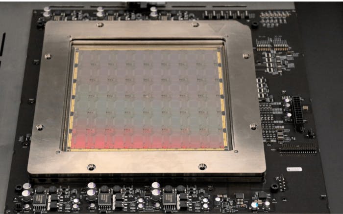
Envise
Source: Lightmatter
Lightmatter's Envise, introduced in 2021, can run neural network computations using integrated electronic and photonic computing technologies to reduce data center power consumption and operating costs. It’s considered to be the world’s first general-purpose photonic AI accelerator, a computer processor designed to speed up AI tasks by using light to process data. Envise is also the first photonic computer for sale that addresses any kind of neural network anywhere from voice assistants to autonomous vehicles along with AI models like OpenAI’s ChatGPT.
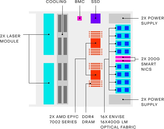
As of 2024, a 16-chip Envise server blade consumes three kilowatts of power, reducing energy usage by 54% compared to equivalent NVIDIA A100-based systems consuming 6.5 kilowatts. Each chip provides 6.4 Tbps of optical interconnect for multi-server scale-out, 1TB of DDR4 DRAM, and 3TB of solid-state memory.
Envise also integrates with PyTorch, enabling machine learning developers to deploy neural networks without modifying their development workflows. Considered to be the world’s first general-purpose photonic AI accelerator, the 4-U Envise server can already process various neural network applications, from voice recognition to autonomous vehicle systems, including large language models.
Source: Nicholas Harris
Idiom
Lightmatter's Idiom software stack enables customers to extract maximum performance on Envise through neural network model compilation and execution. The platform also includes debugging tools (idBug), profiling capabilities (idProfiler), and model optimization features. Idiom's automatic blade detection enables rapid deployment of large AI models across multiple server racks. To start, Lightmatter’s fiber optical communication can link multiple Envise blades together, allowing Idiom to synchronize the Envise chips together in a single runtime.
Idiom then interfaces with deep learning frameworks and model exchange formats through its graph compiler, idCompile. The compiler optimizes deep learning workloads and streamlines neural network programming across multiple Envise blades.
For example, idCompile can automatically divide large neural networks into smaller segments for parallel programming and processing. Through data parallelism, Idiom can instruct multiple Envise units to perform parallel execution of an application or model. idCompile also converts data types to mixed-precision formats whenever possible. This speeds up processing and reduces power consumption without significantly compromising neural network accuracy. Finally, the system can generate an optimized schedule for executing computational operations, reducing latency in the system.
Idiom's idProfiler monitors neural network execution across multiple Envise devices, providing insights into memory usage and performance metrics. These analytics help developers identify model bottlenecks and optimize neural network performance. Another tool, idBug, diagnoses errors in parallel multi-chip operations, streamlining the debugging process. Lastly, Idiom's idML toolkit integrates with PyTorch to optimize neural networks through model compression and quantization while maintaining accuracy. The toolkit supports knowledge distillation between models, enables quantization-aware training, and provides visual analytics for tracking parameter optimization impact on performance.
Market
Customer
The demand for energy-efficient and cost-effective data processing solutions creates three distinct customer segments for Lightmatter's Passage and Envise products: data centers seeking to reduce operational costs, technology companies developing AI applications, and cloud service providers expanding their computing capabilities.
For data centers, Lightmatter uses Passage to enable more efficient data movement between chips or servers, helping companies with data centers to scale generative AI and HPC (high-performance computing) applications. Lightmatter determines the floor plan of a specific chip and layers its silicon photonic chips on it. In 2020, Lightmatter pitched its solution to big data center operators like Amazon and Google to help them get rid of “the giant spaghetti of cables that data center owners use to connect thousands of computer servers.”
AI-driven companies that develop specialized models for their core business operations form the second major customer segment. For instance, healthcare technology companies DeepScribe and Freed deploy AI models for medical transcription services, requiring substantial computational resources. These customers face performance bottlenecks when scaling their AI operations, as simply using more GPUs fails to address the data movement limitations between computing components. The interconnect layer becomes critical for optimal system performance, particularly for companies processing large volumes of industry-specific data through their AI models.
Cloud service providers represent the third major customer segment, as these providers operate computing clusters at a scale where traditional networking infrastructure creates significant bottlenecks. These providers require high-bandwidth connections to support their expanding computational workloads. Lightmatter CEO Harris has observed that cloud service providers “recognize the limitations of traditional networking solutions and the need for efficient, high-bandwidth connections has become paramount.”
Market Size
The global market for AI products and services could reach between $780 billion and $990 billion by 2027, up from $185 billion in 2023.

Source: Bain & Company
More specifically, the global AI hardware market was estimated to be worth $53.7 billion in 2023 and is projected to grow at a 24.5% CAGR until 2033, when it is expected to reach $473.5 billion. In the US, the AI hardware market was estimated to be worth $15 billion and is expected to grow at a 23.9% CAGR to reach $128.7 billion by 2033. Increased adoption of AI, advancements in semiconductor technology, and demand for edge AI solutions are a few forces driving the growth of the AI hardware market.
AI hardware traditionally refers to specialized chips, processors, and computational systems designed to run AI models. The AI inference chip market size, valued at $15.8 billion in 2023, is projected to reach $90.6 billion by 2030 through a 22.6% CAGR. AI inference amounts to 40% of the total AI hardware market and could dominate AI costs in the future because developing more powerful computer chips is a way to boost the performance of an AI model.
Meanwhile, the global photonic integrated circuit market specifically was valued at $8.6 billion in 2023 and is expected to reach $47.6 billion by 2032 at a CAGR of 20.9%. Demand for high rates of electricity from new technologies is the key factor driving this growth. Since incumbent chipmakers like NVIDIA or AMD have an established position in the market, the ability of photonic technology to integrate with existing chips is critical to determine the future viability and growth of the market. Lightmatter claims to be the first company in the photonic computing space, however since photonic computing is not yet widely adopted, the market itself is still at risk.
Competition
Lightmatter's Envise product competes with companies focused on high-performance AI and deep learning hardware, such as NVIDIA H100s, Google TPUs, and Cerebras WSE-3s. These competitors focus on computational speed and energy efficiency for demanding AI workloads. Envise stands out by using photonics instead of conventional electronic transistors, offering greater computational power and lower heat output, which positions it uniquely against these electronic-based accelerators in the AI and high-performance computing markets.
Lightmatter’s Passage focuses on interconnect technology using photonics for high-bandwidth computing systems. The Passage product itself has fewer competitors than Envise since fewer companies are focused on interconnect technologies. Its primary competitor is Ayar Labs.
Photonic Computing Companies
Celestial AI: Celestial AI is a company that specializes in creating high-performance memory and interconnect solutions using silicon photonics technology. Its flagship product, the Photonic Fabric, offers an interconnect solution that allows for ultra-high bandwidth (14.4 Tbps) and low-latency memory transactions. By integrating silicon photonics with chiplet-based architectures, Celestial aims to address limitations in traditional electrical connections and enable faster and more efficient scaling of AI hardware. The technology facilitates memory expansion with reduced energy consumption compared to traditional memory architectures and supports various AI workloads, from machine learning to high-performance computing. Celestial AI’s offerings position itself as a contender in the high-performance interconnect and memory market.
Celestial AI competes with Lightmatter in the photonics and interconnect space, particularly with products like Lightmatter's Passage, which also seeks to address the challenges of interconnect density and bandwidth in large-scale AI systems. While both companies are working on silicon photonics solutions, Celestial AI's focus is more on memory expansion and chip-to-chip connectivity using its Photonic Fabric. In contrast, Lightmatter's Passage is a more comprehensive photonic interconnect platform aimed at scaling AI infrastructure by providing dense optical interconnects between chiplets, along with integrated lasers and switching for dynamic network reconfiguration.
Both companies are pushing towards similar goals in terms of enabling efficient, high-bandwidth interconnects but differ in their approach — Celestial emphasizes memory solutions, while Lightmatter targets broader system-level interconnects for AI and HPC workloads. Celestial AI has raised a total of $338.9 million as of February 2025 from investors including Samsung’s Catalyst Fund, Temasek, and US Innovative Technology Fund valuing it at a valuation of $1.2 billion as of February 2025.
Ayar Labs: Founded in 2015, Ayar Labs specializes in creating optical solutions aimed at enhancing data transfer between server chips. This focus addresses the data transfer inefficiencies which are a significant contributor to increased power consumption in server chips. Similar to Lightmatter’s Passage, Ayar Labs offers its own interconnect technology which also uses photonics to communicate between chips.
Recognizing the potential of Ayar Labs’ technology, NVIDIA invested in the company’s $155 million Series C funding round in May 2023, likely intending to incorporate its optical interconnects into its GPU racks to boost energy efficiency. Ayar Labs then raised a $155 million Series D in December 2024 at a valuation of over $1 billion, with participation from AMD Ventures, Intel Capital, and NVIDIA. As of February 2025, Ayar Labs had raised a total of $374.7 million in funding.
Chip Incumbents
NVIDIA: Founded in 1993, NVIDIA is a full-stack computing infrastructure company with data-center-scale offerings and a market cap of $3.3 trillion as of February 2025. It has captured between 70% to 95% of the AI chip market and the company plans to release a new chip every year as of July 2024. NVIDIA’s “flagship” chip costs ~$30K or more which could give customers an incentive to seek alternatives due to the high price point.
Lightmatter competes with NVIDIA in the AI computing market through its Envise photonic AI accelerator. Envise uses light-based processing to handle the matrix multiplications required in deep learning, potentially offering faster, more power-efficient computing compared to NVIDIA's traditional electronic GPUs (like the A100 and H100). While NVIDIA owns 88% of the market share of electronic GPUs tailored for AI workloads as of June 2024, Lightmatter’s photonics-based Envise is designed to address similar demands in AI while offering advantages in energy efficiency and scalability, potentially positioning it as a viable alternative in data centers and large-scale AI applications.
LLMs will likely continue to get bigger, and as a result, take up more space in memory. NVIDIA GPUs have 80GB of chip memory which is a fraction of what’s required for modern generative AI models that have over a trillion parameters. To meet these memory demands, organizations would need to deploy multiple GPU systems which would increase costs and overhead. In contrast, Lightmatter’s Envise was specifically built to address these challenges by providing a more energy and cost-efficient solution for handling large AI workloads. NVIDIA could also be a customer of Lightmatter as NVIDIA could potentially implement Lightmatter’s interconnectivity product, Passage, into its tech stack. For example, Passage could replace or supplement NVIDIA’s NVLink (high-speed interconnect for GPU and CPU processors) to achieve higher bandwidth and reduced power consumption.
Cerebras: Cerebras Systems is an AI chip manufacturer that builds what the company claims to be “the world’s largest chip”. Its flagship product, the Cerebras Wafer-Scale Engine (WSE), is described by the company as “the fastest AI processor on Earth” which “surpasses all other processors in AI-optimized cores, memory speed, and on-chip fabric bandwidth.” This chip, the size of a dinner plate, offers improved training times and simplified AI training methods at lower prices than Nvidia’s industry-standard GPU chips. Cerebras offers both on-premise deployment and cloud use of its computing systems for companies worldwide seeking to train AI models.”
Cerebras has been pushing the boundaries of speed with its CS-3 system powered by the Wafer Scale Engine 3 (WSE-3). For smaller models, such as the LLaMA 3.1 8B and 70B, Cerebras has set records by delivering 1.8K and 450 tokens per second, respectively. The WSE-3 addresses a critical bottleneck in traditional GPU systems: memory bandwidth. With 7K times more memory bandwidth than NVIDIA's H100, Cerebras eliminates the need to constantly move data between memory and compute cores, allowing faster and more efficient processing, particularly for large-scale models.
Cerebras is focused on solving the memory challenges that limit GPU-based systems, particularly for models requiring substantial memory, such as the LLaMA 70B, which needs 140 GB of memory. For even larger models, Cerebras employs a solution by splitting models across multiple CS-3 systems, enabling it to handle models ranging from billions to trillions of parameters. Both Cerebras and Lightmatter aim to transform AI processing, with Cerebras focusing on wafer-scale electronics and Lightmatter on photonic solutions. Their competition centers around providing energy-efficient, high-speed solutions for the data-heavy requirements of AI, although they take fundamentally different technological paths to get there.
Business Model
As of February 2025, Lightmatter’s pricing model isn’t publicly available. However, by embedding optical interconnects directly into chip packaging, Lightmatter aims to dramatically improve the performance and efficiency of data center architectures. This would enable data centers to scale with the growing demands of AI workloads. Lightmatter’s revenue model is likely centered on both direct product sales and long-term partnerships with enterprises that require cutting-edge computing solutions. Harris has stated that the price point for Envise is “pretty competitive with standard silicon although extreme performance might command some premium.”
Lightmatter may also offer licensing or technology integration opportunities, particularly for large-scale infrastructure deployments where photonic solutions can optimize data movement and processing efficiency. The growing trend toward cloud and AI-focused data centers could represent significant monetization opportunities. Lightmatter’s business could also benefit from the increasing trend of adopting silicon photonics in next-generation AI chips and systems, positioning Lightmatter to capitalize on a potential shift in the market away from traditional electronic-based architectures.
Traction
Lightmatter works with semiconductor companies including AMD, NVIDIA, Intel, and Qualcomm to put their chips on top of Lightmatter’s optical interconnect substrate. Lightmatter’s CEO has stated that Lightmatter’s substrate is “the foundation for how computing will make progress. It’ll reduce the energy consumption of these clusters dramatically and it will enable scaling to a million nodes and beyond [which] is how you get to wafer-scale, the biggest chips in the world, and AGI.” On typical workloads, Lightmatter is up to 10x faster than technologies like NVIDIA’s A100 chip. Moreover, it gets eight times the throughput of an NVIDIA server blade using one-fifth of the power. As of February 2025, Lightmatter had an estimated 191 employees between its two offices in Boston and Mountain View, a 46% growth in employees from 2023.
In November 2024, Lightmatter partnered with Amkor Technology, a leading provider of semiconductor packaging and test services, to build the world’s largest 3D-packaged chip complex utilizing Lightmatter’s Passage. Lightmatter’s photonic technology coupled with Amkor’s multi-die packaging expertise could help meet the interconnect scaling and power demands of AI workloads.
Multi-die chip packaging can divide a large semiconductor chip into smaller dies, enabling multiple individual dies within a single package. This technology, when combined with Lightmatter’s photonic technology, could reduce the energy required for data transfer between components by using light-based interconnects within the multi-die package. Ritesh Jain, SVP of engineering and operations at Lightmatter, stated that the partnership would be “a pivotal step in building a world-class ecosystem that empowers our customers to realize AI and HPC compute offerings with unprecedented bandwidth and efficiency.”
Valuation
In October 2024, Lightmatter raised a $400 million Series D round at a $4.4 billion valuation led by T. Rowe Price with participation from previous investors Google Ventures and Fidelity. This brings it to a total of $822 million raised across six funding rounds from previous investors including Matrix, Spark Capital, SIP Global Partners, Sequoia, Lockheed Martin Ventures, FAST (by GettyLab), Hewlett Packard Enterprise, Viking Global Investors, Trajectory Ventures, and Eastward Capital Partners.
Harris has stated that Lightmatter’s Series D was most likely the last funding round it would raise. In October 2024, he also hinted that Lightmatter had booked large deals which is the reason that it was able to receive the level of funding that it did.
Key Opportunities
Market Positioning
The deceleration of Moore's Law and the physical limitations of silicon chip manufacturing create an immediate opportunity for photonic interconnect technology in high-performance computing. As silicon-based chips reach their physical and economic limits, data centers require new solutions to process growing AI workloads. Lightmatter's photonic technology addresses these constraints through faster data transport and reduced energy consumption, providing the infrastructure needed for large-scale chip interconnection in modern data centers.
By leveraging photonics, Lightmatter can capitalize on the rising need for AI infrastructure that supports interconnect-dense environments. Passage aims to seamlessly integrate with maximum-sized chips, potentially approaching wafer scale, to create unified systems that treat entire data centers as single, high-power computers. This opportunity aligns with the push to develop artificial superintelligence, where Lightmatter’s photonic interconnects could become the technology driving AI to new performance frontiers. NVIDIA’s GPUs and Intel Xeon CPUs are growing at CAGRs of 13% and 18% respectively which could lead them to wafer-scale by 2040. The number of interconnections scales 4x with each chip leading to routing, bandwidth, and latency challenges. Light could be the solution to that problem.
New Substrates for Chips
In addition to interconnecting chips, Lightmatter is reportedly developing new substrates for chips to try and help them perform even more intimate networking tasks using light. As of October 2024, Lightmatter CEO Nicholas Harris believed that in 10 years, wafer-scale chips like those pioneered at Cerebras will become the industry standard. However, he believes that Cerebras isn’t able “to capture the true value of that advance in this [early] stage of the technology.”
Substrates for chips are foundational materials that house and support microelectronics, enabling connections between the chip's delicate circuits and the larger system. They play a vital role in maintaining chip stability, electrical performance, and thermal management. In the future, advanced substrates could be an opportunity for Lightmatter as it scales its photonic technology. By developing and utilizing next-generation substrates, Lightmatter could integrate larger and more complex photonic components, like wafer-scale chips, which could enhance performance, reduce latency, and support the massive interconnect demands of AI and ASI data centers.
Laser Technology
The development of chip-scale erbium-doped waveguide lasers presents an intriguing opportunity for Lightmatter. Erbium-doped lasers, traditionally used in fiber optics, incorporate erbium ions, atoms of the element erbium that have lost some of their electrons, giving them a positive charge, as a gain medium to amplify light at specific wavelengths with high coherence and stability, crucial for long-distance and precise optical applications. As a company producing photonic computing and interconnect solutions, Lightmatter could leverage these miniaturized, highly stable lasers to enhance their photonic data processing and interconnect products.
Integrating erbium-based fiber lasers could improve the precision, energy efficiency, and scalability of Lightmatter’s products, particularly for high-bandwidth data centers and AI workloads that demand reliable and low-latency connections.
Additionally, this technology could align with Lightmatter's focus on overcoming traditional electrical interconnect limitations. The miniaturized laser technology would allow Lightmatter to develop more compact, high-performance photonic chips, potentially reducing costs and increasing compatibility with existing semiconductor manufacturing processes. This could also open pathways for Lightmatter in industries like telecommunications, LiDAR, and advanced sensing, where stable, chip-scale lasers are increasingly valuable.
Key Risks
Photonic Computing Adoption
The integration of photonic computing into existing electronic systems presents significant technical challenges. Manufacturing and design complexities inherent to light-based technologies create barriers to customer adoption as of 2024. While Lightmatter states its technology integrates with existing electronic infrastructure, the absence of publicly announced customers indicates potential market hesitation toward adopting this novel approach. This adoption risk increases for data centers with established electronic systems due to operational disruption concerns.
Logic Operations
Photonic computing faces fundamental constraints in executing logic operations, particularly in general-purpose computing tasks that require control flows and conditional statements. Historical attempts to overcome these limitations, such as Bell Labs' optical transistor development in the 1980s, failed due to the complexity of nonlinear light beam interactions. Lightmatter addresses this constraint by focusing exclusively on linear algebra computations, which align with electromagnetic properties. This specialized focus limits the technology's applications to specific fields including machine learning, aerospace engineering, chemistry, and quantum computing.
Summary
The increasing computational demands of AI systems are pushing traditional silicon-based computing toward its physical and economic limits. As Moore's Law decelerates, data centers and AI companies seek new solutions to process growing workloads while managing energy consumption and operational costs. Lightmatter addresses these challenges through its photonic computing hardware, which uses light instead of electrical signals for calculations. The company's flagship product, Passage, provides a photonic interconnect solution that integrates with existing data center infrastructure to enable higher bandwidth data movement and reduced power consumption for chips, while its secondary product, Envise, is a photonic AI accelerator to run energy-efficient AI computation.