Actionable Summary
The correlation between territorial size and geopolitical power is one of history's most enduring patterns. At their respective peaks, the Roman Empire controlled 2 million square miles, the Mongol Empire commanded an unprecedented 9.3 million square miles, and the British Empire ruled over roughly 25% of Earth's landmass.
This pattern persists today as the world's most consequential powers, from America to Russia, China, and India, derive significant advantage from their geographic scale and resource abundance. These world superpowers are also four of only nine nations with nuclear weapons, now undergoing rearmament as great power competition intensifies for the first time in nearly 40 years.
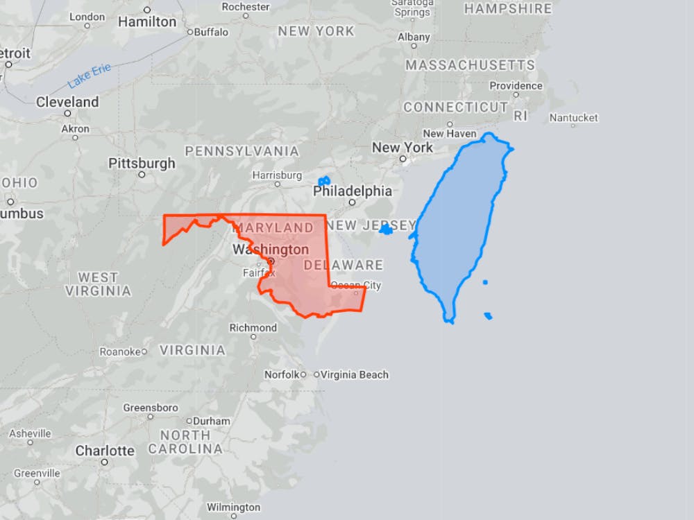
But against historical precedent, just one relatively small nation commands comparable influence to the world’s superpowers. At just 13,976 square miles, slightly larger than the state of Maryland, Taiwan is paradoxically the most important and contested hotspot in the geopolitical landscape today, with Washington, Moscow, and Beijing all developing strategic plans around the island's future.
By far the primary reason behind the island’s disproportionate global influence stems from a single company: Taiwan Semiconductor Manufacturing Company (TSMC). Within its borders, TSMC manufactures close to 92% of the world’s most advanced semiconductor chips. While aligned with the US strategically, Taiwan is only 110 miles from China’s coast. China has also increasingly asserted territorial claims over the island.
Today, roughly 70% of electronics are manufactured in Asia. It’s easy to lump in the story of semiconductors with the rise of Asian manufacturing, but the original birthplace of the semiconductor industry is on American soil. In 1947, American physicists John Bardeen, Walter Brattain, and William Shockley invented the first transistor at Bell Laboratories. From there, the transistor rapidly evolved, mirroring the rise of globalization as large companies outsourced increasing volumes of production to foreign manufacturing.
In 1955, Shockley left Bell Labs to establish Shockley Semiconductor to commercialize the transistor. While Shockley Semiconductor would quickly end up being a commercial failure, it’s credited with bringing together the most talented semiconductor physicists of the era, known as the Traitorous Eight, who would go on to create Fairchild Semiconductor, Intel, AMD, and dozens of other generational semiconductor companies in the US.
Each American semiconductor company originally built its own semiconductor fabrication plants (also known as foundries) in the US. In the 1990s, Jerry Sanders declared boastfully, “real men have fabs.” But over time, foundry buildout slowed and eventually reversed, as it grew increasingly unfeasible to maintain foundries due to the pressure of exponential adoption and rapid miniaturization. As the market matured, only the largest semiconductor companies could sustain leading internal foundries. Today, Intel remains the only American company that maintains a leading-edge foundry on American soil.
The original business model of semiconductor manufacturing had been dominated by integrated device manufacturers (IDMs) who controlled the end-to-end value chain of a chip from design to manufacture and sale. However, the increasing complexity of each new generation of chip, the lower cost of manufacturing in Asia, and the rapidly accelerating capabilities of Asian manufacturers drove a wedge in the middle of the semiconductor manufacturing industry that resulted in two kinds of companies: the fabs and the fab-nots.
In the 1980s, the prevailing belief was that companies could outsource foundry services to cheaper, overseas options. If the US focused on the more intellectually demanding aspects of chip design while outsourcing the lower-skill manufacturing work abroad, it would be “a success.” As such, the US’s share of global chip fabrication fell from 100% in the 1960s to 37% by 1990. By 2024, that number had further dwindled to just 8%.
Andy Grove, the first employee at Intel and its third CEO, disagreed with this belief. In 2010, Grove explained in hindsight the damage this type of offshoring did: “We broke the chain of experience that is so important in technological evolution… Abandoning today’s ‘commodity’ manufacturing can lock [us] out of tomorrow’s emerging industry.”
For the first two decades of the 21st century, most American companies didn’t see dependence on TSMC for the majority of semiconductor fabrication as a problem. But chip shortages from COVID-19-related supply chain disruptions in 2021 and the frenzy for AI chips after 2022 have changed the prevailing opinion. Suddenly, everyone realized it was a problem important enough to be considered a national priority.
The next battleground in the emerging Cold War II with China will be in AI. But without access to leading-edge chips to run these AI models, the West’s ability to lead in AI capability and leverage it for geopolitical security will be severely affected. The singular dependence on this tiny island and TSMC has created a dangerous chokepoint for America. This is an urgent and unacceptable vulnerability that will threaten both our national security and technological edge. The question now isn't whether America needs its own TSMC, but how we’re going to build one.
The majority of this piece will unpack three options to address this critical vulnerability: do we build an American Semiconductor Manufacturing Company from scratch, borrow it from TSMC’s expertise, or “buy it” from an existing player with the right capabilities? Our conclusion is that there is only one realistic option: Intel is an unavoidable piece of the puzzle to rebuild America’s domestic semiconductor manufacturing capacity.
Dylan Patel, a semiconductor analyst and founder of SemiAnalysis, has asserted that “Intel Foundry’s survival is key to America’s national and economic security as the only domestic company with advanced logic R&D and manufacturing capability.”
The re-industrialization of a successful Intel Foundry has been stymied by two core forces: (1) the gradual replacement of the traditional engineering-centric culture with a management-centric culture, resulting in inferior fabrication capabilities, and (2) an ongoing conflict of interest between internal fabrication capability and external design partners that Intel has consistently tried to ignore. Only in the last few years has it become readily apparent that something has to change. Intel is staring down the barrel of the innovator’s dilemma, and it no longer has the option of doing nothing.
The history of the semiconductor is the history of the United States. From inventor, to manufacturer, to consumer, to hostage. The US has had a complex relationship with the semiconductor industry historically. Going forward, it will remain the single most important building block upon which American technological independence will live or die. The only solution to dig ourselves out of our current vulnerabilities is by building an American Semiconductor Manufacturing Company (ASMC) from the existing Intel Foundry business.
Despite Intel’s central role in this thesis, it’s not the only part of the solution that needs to be built to secure our technological independence. ASMC is an ideal that will require an entire ecosystem to realize, including the support of the US government in funding and incentivizing domestic talent for American semiconductor manufacturing, a loyal base of American technology companies willing to commit to American semiconductor capacity, Intel Foundry leading the charge in building back American capability, and new-age startups building new chip designs, investigating semiconductor materials, and new computing paradigms.
This is an overview of a critical space and evolving story, but it’s not exhaustive. Our research is built on the back of some exceptional contributors to this conversation, including Dylan Patel and the team at SemiAnalysis, Dan Nystedt, Palladium, Institute For Progress, Raja Koduri, Dwarkesh Patel, Ben Thompson at Stratechery, Austin Lyons at ChipStrat, Asterisk, as well as authors like John Lewis Gaddis, Chris Miller and many others.
Taiwan, Chips, & Cold War II
Imagine a nation of just 13,976 square miles, slightly larger than the state of Maryland. In a world where nations stockpile nuclear weaponry and edge towards great power conflicts, how big of an impact could one little island make?
It turns out, quite a big one. A place that appears insignificant in size may well be the biggest geopolitical flashpoint in the modern world: Taiwan.
Source: Bubble Tea Island
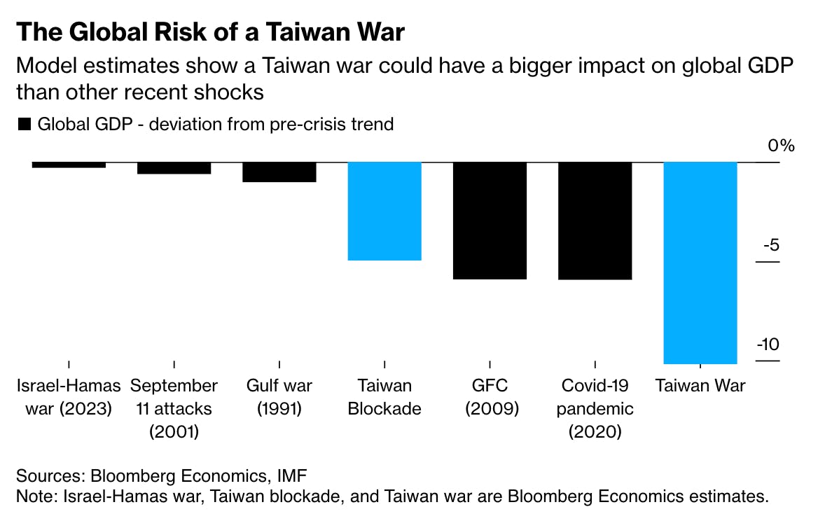
To quantify its economic importance, a large-scale conflict over Taiwan and the resulting shutdown of Taiwan Semiconductor Manufacturing Company (TSMC) could result in an estimated $10 trillion global economic collapse and wipe out 10% of global GDP overnight.
Source: Bloomberg Economics
Waging war over a scarce resource is nothing new. Salt, tea, and oil have all sparked their fair share of conflict. However, while transformational technologies like gunpowder have historically provided decisive, yet temporary, advantages, the first Cold War marked a new paradigm of conflict, as it was defined by a singular capability that could single-handedly decide the outcome of any conflict: nuclear weapons.
As the Cold War evolved, the battleground centered around the ever-advancing capability of sophisticated nuclear delivery systems, from nuclear submarines in 1955 to the Space Race in 1969, and ending with the “Star Wars” missile defense program in 1983; all of which aimed to expand intercontinental strike capability. But nuclear buildup required one of two foundational resources: enriched uranium-235 or plutonium-239. Without them, it wasn’t possible to make nuclear weapons.
Although the first Cold War ended with the fall of the Berlin Wall and the dissolution of the Soviet Union in the 1990s, a new conflict has emerged between China and the US that has been dubbed Cold War II, which parallels the first in many respects.
The underlying dynamics, for example, remain the same: to be the first nation to develop a technology that will yield an absolute, permanent advantage. That technology is Artificial General Intelligence (AGI).
AGI could trigger an exponential intelligence explosion, initiating self-improving research to discover novel materials for fighter jets, formulate unbeatable wargaming strategies, command autonomous drone fleets with superhuman efficiency, and unlock revolutionary scientific breakthroughs for warfare. As a result, the first nation to reach AGI and fully unlock its potential would have a decisive advantage. And just as the nuclear arms race in Cold War I relied on foundational resources like plutonium and uranium, Cold War II will rely on the foundational resource that makes AGI possible: advanced semiconductors.
The importance of AI has been clear to adversaries of the US for some time. In 2017, Vladimir Putin laid out the criticality of AI from his perspective: “Whoever becomes the leader in [artificial intelligence] will become the ruler of the world.” By 2018, China spent more money on importing semiconductors than it did on importing oil.
China invested almost $1 trillion into strategic categories like AI from 2014 to 2024 and is now closely trailing the capabilities of US frontier AI labs. China’s release of DeepSeek-R1 in January 2025, a reportedly cheap, open-source, performant AI model, has been called a Sputnik moment in this new Cold War. Mirroring the Sputnik launch 70 years ago, DeepSeek showed the world that a committed geopolitical opponent had leapfrogged (albeit temporarily) the US in AI superiority.
The closing of the AI gap between the two contestants of Cold War II places a level of strategic importance on advanced semiconductors that is difficult to overstate. It would not be an exaggeration to say that whoever controls this foundational resource of AI will be the winner of the second Cold War.
That’s where Taiwan comes in. By far the biggest reason for the island’s disproportionate geopolitical importance is a single company: TSMC. Within Taiwan’s borders, TSMC manufactures close to 92% of the world’s advanced semiconductor chips, which are critical for AI-related applications. While politically aligned with the US, Taiwan is only 110 miles from China’s coast, an adversarial nation that has continuously asserted territorial claims over the island.
Semiconductors are classified as either leading-edge or legacy nodes. Leading-edge chips are those built using new, advanced processes that can print transistor features as small as 2nm onto a silicon wafer. In principle, smaller transistors translate to faster processing speeds, lower power consumption, and expanded functionality, which is why leading-edge chips almost exclusively power the latest AI models, computers, and smartphones.
Legacy nodes, conversely, feature much larger transistor sizes, often 28nm or higher. These are significantly cheaper and easier to produce and are thus used in common electronics like cars and everyday appliances, where ultra-high performance isn’t necessary. Access to legacy nodes remains crucial for producing any electronic devices we might need. But without access to advanced nodes, it becomes almost impossible to build frontier AI models.
This distinction is important to note. While Taiwan produces roughly 67% of all global semiconductors, Taiwan dominates the advanced node sector. This is the key bottleneck for both the US and China in their race to AI. Beyond that, semiconductor supply chains have implications that extend beyond AI, and if those supply chains were to be cut off, it would directly affect the US military's operational capacity.
Advanced and legacy node semiconductors are, for example, increasingly used in every critical weapon the US military relies on. Precision guided missiles, F-35 fighter jets, or UAVs, and virtually any modern military system that relies on sensors, radar, guidance systems, or cameras will contain an advanced semiconductor chip.
Without access to the semiconductors from Taiwan, US military power will be directly impacted. We would be incapable of developing advanced AI, let alone pursuing AGI, and anyone who did have access to AGI would have a compounding advantage against us. We would also be unable to assemble most of the advanced technology that has become a critical part of a modern military. Taiwan, therefore, represents a massive single point of failure across consumer, enterprise, and military applications.
In this deep dive, we explore how America got itself into this predicament. How did we let the foundation upon which our future is built get put at such risk? And how can America avoid its continued geopolitical dependence on Taiwan?
Our answer is that the only way to extricate ourselves from the current predicament is for America to build an American Semiconductor Manufacturing Company. To understand how and why, we have to first understand how we got to this point.
The Golden Age of American Semiconductors
Anything remotely electronic contains, at minimum, a single semiconductor chip, from systems like phones and computers, to devices we take for granted like rice cookers and LED light bulbs.
Given the fact that more than 70% of electronics are manufactured in Asia, it’s easy to lump in the story of semiconductors with the rise of Asian manufacturing. But we forget that the semiconductor was invented on American soil, and that it was foundational to much of the US’s tech industry in the decades since. The internet, personal computing, mobile phones – every aspect of technological innovation over the last 100 years was built on the foundation of semiconductor technology.
Transistors: The Building Blocks of Semiconductors
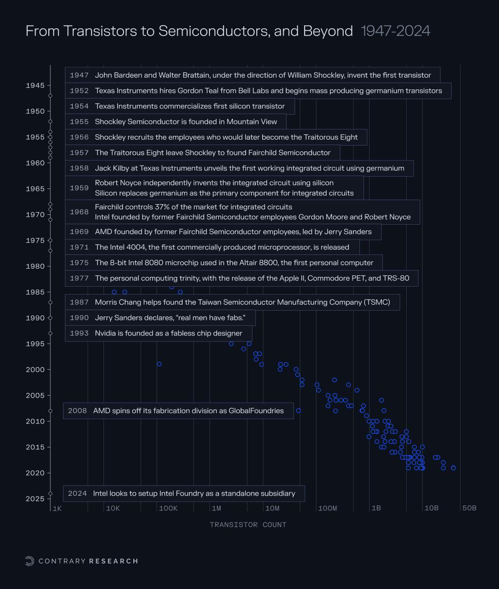
The key breakthrough that led to the semiconductor revolution came with the invention of the transistor in 1947 by American physicists John Bardeen, Walter Brattain, and William Shockley. Developed at Bell Laboratories, the bipolar point-contact transistor offered a smaller, more reliable, and energy-efficient replacement for vacuum tubes, which were the earliest form of electronic circuits.

Source: Computer History Museum
The term ‘transistor,’ coined by Bell Labs engineer John R. Pierce, came from the combination of the words “transfer” and “resistor,” describing the device’s operational principle. Transistors work by using a small input voltage or current to control a larger current flowing between two terminals, acting similarly to a variable resistor whose resistance changes based on the input signal.
From the year of its invention, the transistor rapidly evolved, mirroring the rise of globalization as large companies outsourced increasing volumes of production to foreign manufacturing.
Source: Our World In Data; Contrary Research
While the team at Bell Labs would win the Nobel Prize in 1956 for their work, it wouldn’t be Bell Labs that ultimately commercialized transistors. Instead, it was Texas Instruments (TI) who did, after obtaining a license from Bell Labs’ parent company, AT&T, for just $25K. Founded in 1951, the company began mass-producing germanium transistors less than a year later.
The initial commercialized transistors were manufactured with germanium, but this semiconducting material faced significant limitations, like high leakage currents and a low tolerance for heat. Recognizing these limitations early on, TI transitioned from producing germanium transistors to commercializing the first silicon transistor in 1954. Silicon was more reliable and, most importantly, easier to reliably mass-produce. This solidified silicon as the semiconducting material of choice for the next 70 years. But the future of computing wasn’t built at TI, which manufactured standalone transistors. Instead, it would be Shockley Semiconductor that built the silicon integrated circuit.
Silicon Valley & Silicon Integrated Circuits
In 1955, Bell Labs alumnus William Shockley, who had directed the team that invented the original germanium transistor, established his own operation: Shockley Semiconductor Laboratory. An aging mother and an affinity for Caltech led Shockley to set up shop not in the hub of manufacturing on the East Coast alongside Bell Labs, GE, and IBM, but in Palo Alto.
Silicon Valley was born.
While Shockley Semiconductor would end up being a commercial failure, it’s credited with bringing together one of the most important groups of people in the history of technology: the Traitorous Eight. Given Shockley’s reputation at Bell Labs for being a maniacal manager, he had a hard time recruiting, and convincing people to move to California wasn’t easy either.
Shockley placed an ad in the New York Times and Palo Alto Times. Out of approximately 300 responses, Shockley narrowed it down to 32 employees by September 1956. Some of the people who responded to the ad included Jay Last, a former intern at Shockley’s early investor, Beckman Instruments; Gordon Moore, a Ph.D. from MIT and Johns Hopkins; Robert Noyce, from Philco; Victor Grinich from Stanford, and Sheldon Roberts from Dow Chemical. Others were recruited by Shockley directly, including Julius Blank and Eugene Kleiner, from Western Electric, a Bell Labs sister company, and Jean Hoerni from Caltech.
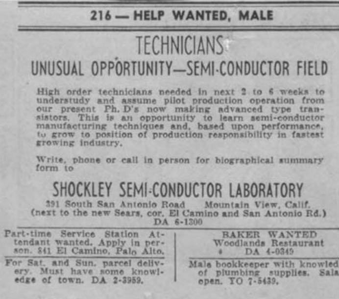
Source: Palo Alto Times
Those eight employees would barely last a year. After putting up with intense paranoia from Shockley, including recorded phone calls, limited internal collaboration, and mandatory lie detector tests, the eight defected and set out on their own. In September 1957, Fairchild Semiconductor was created.
In early 1959, Robert Noyce, of the Traitorous Eight, developed an integrated circuit (IC) using silicon. Almost simultaneously, in late 1958, Jack Kilby, an employee at TI, had also developed the integrated circuit, albeit using germanium rather than silicon. The IC enabled multiple transistors, resistors, and capacitors to be etched onto a single silicon chip, drastically reducing both the size and complexity of electronic circuits. This miniaturization allowed the production of much smaller, lighter, and more efficient devices, paving the way for portable electronics and computing.
While Jack Kilby, not Robert Noyce, was later awarded the Nobel Prize for the integrated circuit, it was Fairchild Semiconductor that dominated the market for integrated circuits. At its peak in 1968, Fairchild controlled 37% of the integrated circuits market after having pushed the first commercial silicon transistors to mass production in 1959.
The majority of early vacuum tube research was funded by the US military, and the same became true for the integrated circuit. The US Air Force and NASA were the main consumers of ICs in the 1950s and 1960s for their lunar missions and precision-guided Minuteman II missiles during the Vietnam War. Over 50% of R&D funding was subsidized by the government, effectively giving birth to the entire industry. At one point, 80% of Fairchild’s revenue came directly from the military. Leslie Berlin, project historian for Stanford’s Silicon Valley archives, also pointed out that “100% of the early microchips went to defense use.”
Eventually, the integrated circuits that made their way into almost every military use case started to catch on in commercial markets. In 1968, Fairchild alumni Gordon Moore and Robert Noyce started Intel with an explicit focus on working not just with the military, but the budding consumer market too. They envisioned an “even larger civilian market for chips, though in the early 1960s no such market existed.”
But that market was coming. The development of metal–oxide–semiconductor (MOS) chip technology eventually led to the first commercially produced microprocessor by Intel. The Intel 4004, released in 1971, was largely utilized in business calculators. As microprocessors became smaller and mass production made them more affordable, the stage was set for the personal computer revolution of the late 1970s and 1980s. The Intel 8080 microchip was used in the Altair 8800 in 1974, considered by many to be the first personal computer.
In 1977, personal computing experienced the birth of its own trinity: the release of the Apple II, Commodore PET, and TRS-80; all produced by American companies. Standing at that moment in time, it would have been easy to believe American technological dominance was just getting started. Unfortunately, the opposite was true, at least as it related to semiconductor manufacturing.
The groundwork was already being laid for America’s gradual, then sudden, decline.
The Decline of American Dominance in Semiconductors
A little over a decade after the Traitorous Eight set up shop at Fairchild Semiconductor, another group of eight defectors started another semiconductor manufacturing operation, though this time the defectors came out of Fairchild rather than into it. Led by Jerry Sanders, a rising marketing star at Fairchild, the group started their own company in 1969 called Advanced Micro Devices (AMD). Sanders personified the “macho-man posturing” of American semiconductor manufacturing prevalent during the 1980s and 1990s, while ironically, domestic capability was quietly being undermined.
Historically, American semiconductor companies operated under the integrated device manufacturer (IDM) model, in which companies controlled the end-to-end value chain of a chip from design to in-house fabrication. These fabrication plants (also called fabs or foundries) were a point of pride in the US, a sentiment famously embodied by Jerry Sanders’ 1990s boast, “real men have fabs.” But over time, foundry buildout slowed and eventually reversed, as it grew increasingly unfeasible to maintain foundries due to the pressure of exponential adoption and rapid improvement of semiconductors:
Exponential Adoption: In 1966, when the use cases were still largely defense-driven, sales of semiconductors passed $1 billion. By the 1990s, semiconductors had become ubiquitous both in personal computing, with IBM and Apple, and in consumer electronics like VCRs, video games, and more. That led to semiconductor sales reaching $100 billion by 1994. In 2021, that number reached $555 billion with over 1.15 trillion semiconductors sold globally.
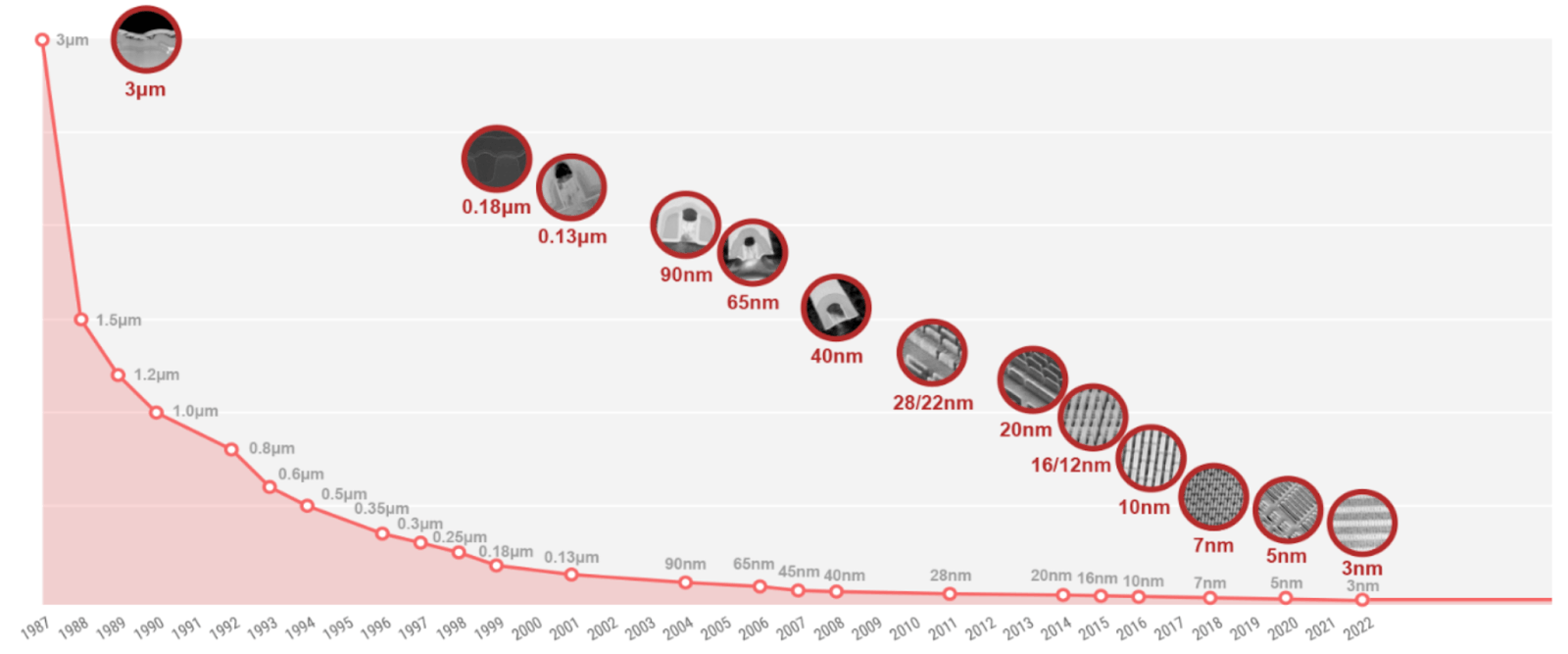
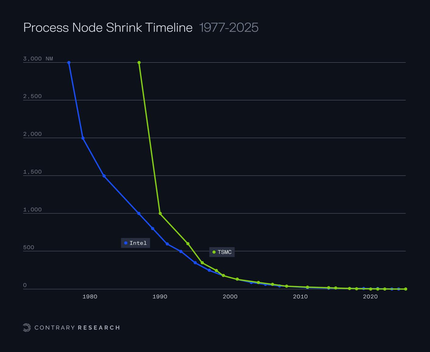
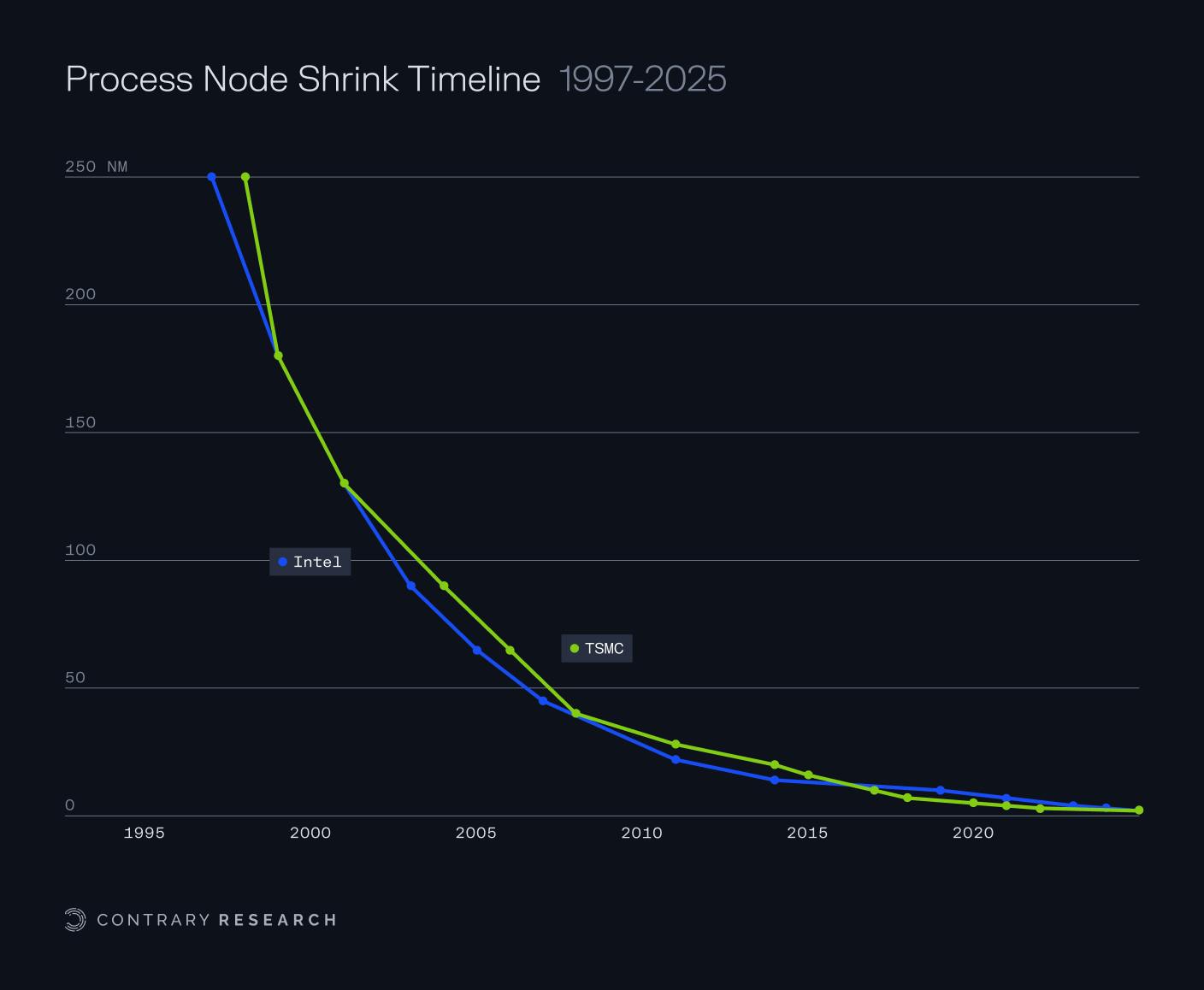
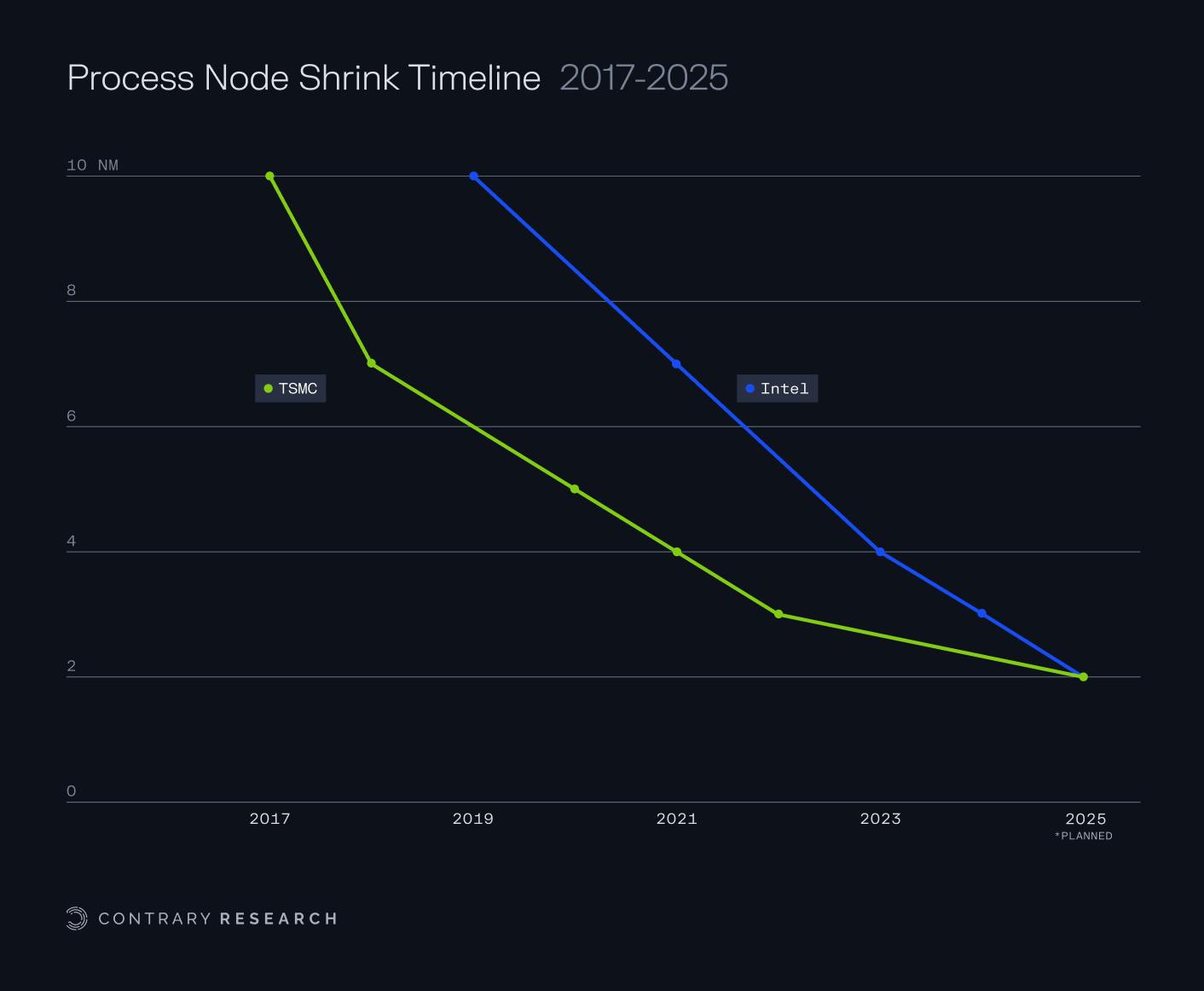
Rapid Improvement: The quintessential framework in the semiconductor industry is Moore’s Law, the prediction in 1965 by Gordon Moore that every year the number of transistors in an integrated circuit would double (revised to every two years in 1975). That rate of improvement held true until 2016. While that rate may not be doubling every two years, the rate of progress is still meaningfully fast. Companies like TSMC and Intel have plans for the production of 2nm and 1nm chips in 2025 and 2027, respectively.
Source: TSMC
These two factors compounded to put immense pressure on the traditional manufacturers of semiconductors. As the global demand for semiconductors continued to explode and the technical sophistication of each new generation of chips became more complicated, manufacturers began to look for ways to extend their capabilities.
The first approach was classic offshoring, just like other industrial categories, from textiles to automotive. As far back as 1963, Fairchild signed a licensing agreement with Nippon Electric Company (NEC) in Japan to manufacture relatively simple, discrete semiconductor components, such as transistors and basic logic integrated circuits. Robert Noyce himself visited the company in 1963.
Over the course of the 1960s and 1970s, other companies followed suit, including RCA, Texas Instruments, Intel, and Motorola, which partnered with Asian firms Hitachi, Toshiba, Samsung, and Fujitsu to manufacture semiconductor components. It’s important to note that, at first, the components being offshored were not the leading edge of the manufacturing industry. These were simple discrete transistors, diodes, logic gates, and basic memory components, meant to simply alleviate the pressure of rapid adoption to increase capacity. Offshore partners would build the simple components, giving American semiconductor manufacturing companies the capacity to focus on the leading-edge.
One key turning point was the competition over Dynamic Random Access Memory (DRAM) chips in the 1980s. DRAM memory was invented at Intel in the 1970s, but was ultimately forced to exit the business 14 years later in 1984 when the company failed to compete with Asian manufacturers. By this point, semiconductor foundries in Asia had built up so much semiconductor manufacturing capability that they could more readily compete for more advanced technologies like DRAM chip manufacturing. The pursuit of more capacity from US semiconductor manufacturers had inadvertently given their Asian partners just the experience they needed to compete with those very manufacturers and turn into rivals.
As a result, domestic chip fabrication in the US fell from 100% in the 1960s to 37% by 1990. But this actually was seen as a positive development. The prevailing belief was that companies could outsource foundry services to cheaper, overseas options. If the US focused on the more intellectually demanding aspects of chip design while outsourcing the lower-skill manufacturing work abroad, it would be “a success.” Andy Grove, the first employee at Intel and its third CEO, disagreed. In 2010, Grove explained in hindsight the damage that offshoring did to the industry:
“We broke the chain of experience that is so important in technological evolution. As happened with batteries, abandoning today’s ‘commodity’ manufacturing can lock [us] out of tomorrow’s emerging industry.”
That is exactly what has happened. Even Jerry Sanders backtracked his position of “real men have fabs” and divested their in-house foundries to form what is known today as GlobalFoundries in 2009. As Chris Miller explained in Chip War, “it became harder to make money while owning and operating a fab. Each generation of technological improvement made fabs more expensive.” The increasing complexity of each new generation of chip, the lower cost of manufacturing in Asia, and the rapidly accelerating capabilities of Asian manufacturers drove a wedge in the middle of the semiconductor manufacturing industry that resulted in two kinds of companies: the fabs and the fab-nots.
Today, the fab-nots dominate the US, while domestic chip fabrication has further dwindled to just 8% of global capacity.
The Fabs & The Fab-Nots
In 1958, when the Traitorous Eight were just beginning their work at Fairchild and before the era of Intel and AMD, Morris Chang joined Texas Instruments (TI) and grew to eventually lead its offshoring efforts. In 1968, Chang first visited Taiwan to evaluate its potential for a TI factory.
Members of the Taiwanese government saw the criticality of working with American manufacturing companies. Leading that effort was Li Kwoh-Ting, Taiwan’s economic minister at the time. Facing an increasingly hostile China, Li believed that even if Americans weren’t interested in defending Taiwan, they “might be willing to defend Texas Instruments,” a strategy that later came to be known as Taiwan’s silicon shield. Li convinced Chang to offshore TI’s foundries in Taiwan, and in August 1969, the first Taiwanese TI plant was built. By 1980, it delivered its billionth transistor unit.
But Li wanted Chang to do more than just support Taiwan through TI as a proxy. In 1985, Li asked Chang to “lead Taiwan’s chip industry” and “promote a semiconductor industry in Taiwan,” regardless of capital costs. Fortunately for Li, since the mid-1970s, Chang had been considering the idea of building a semiconductor foundry that would only manufacture chips designed by other companies without designing its own. Now was his chance to do it with the backing of a nation with a $63 billion GDP. That was 20x the market cap of Texas Instruments at the time. Chang had left TI in 1983, frustrated at institutional inertia, which allowed Chang to seriously consider Li’s proposal. In 1985, Chang agreed to lead Taiwan’s Industrial Technology Research Institute, setting in motion the most consequential industrial bet in modern East Asian history, which eventually became the semiconductor giant we know today as the Taiwan Semiconductor Manufacturing Company (TSMC).
While some firms of that era, like Intel and Texas Instruments, remained as IDMs, the new standard in the semiconductor industry by the 1980s was to become a fabless chip designer. No longer was owning fabs a point of pride if you could switch to cheaper manufacturing elsewhere. Fabless chip designers would do the research and development required to invent at the leading edge of chip capability. But then, instead of manufacturing in-house, they would turn to pure-play foundries, like TSMC, for less expensive manufacturing.
Under the pure-play foundry model, Chang’s TSMC would grow to outperform the prevailing IDM model. By exclusively dedicating itself to the fabrication of semiconductors for other chip design firms, TSMC could serve many fabless design companies. This aggregation of demand would enable TSMC to achieve immense production volumes, which, in turn, would create manufacturing efficiencies that a single in-house foundry could not replicate.
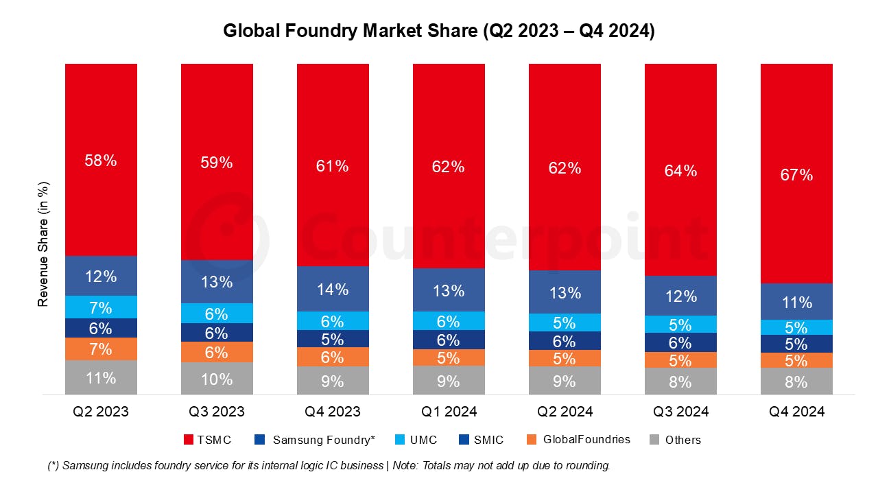
While the US market share of semiconductor manufacturing dropped from 37% in 1990 to 10% in 2024, Taiwan grew from basically zero to 22% over the same time frame, which accounts for more than the US and Europe’s market share combined. As of Q4 2024, TSMC controlled roughly 67% of the global semiconductor foundry market and supplies 92% of the world’s advanced chips.
Source: Counterpoint Research
Chang first envisioned this pure-play foundry business after being exposed to learning curve theory in the late 1960s. This principle, sometimes referred to as Wright’s Law, states that production costs inherently decrease by a consistent percentage with every doubling of cumulative production volume. Consequently, Chang's TSMC pure-play foundry, by virtue of serving many clients and aggregating industry demand, can scale its production volume, translating to reduced production costs.
But demand for a business model like pure-play foundries depended on the emergence of fabless semiconductor companies, which didn't exist in the market at the time. In 1984, only Xilinx operated on a fabless model. But that wouldn’t last for long: after TSMC’s founding in 1987, numerous firms adopted the fabless model: Altera, Qualcomm, Cirrus Logic, and, most importantly, Nvidia in 1993.
Just as so many saw offshoring as a win, the economic model in semiconductor manufacturing was once again overturned in favor of this new dynamic between pure-play foundries, like TSMC, and fabless chip designers like Nvidia. As Chris Miller described in Chip War, the new guard of semiconductor leaders had a meaningfully different tone about what part of the business they were most focused on:
“The new class of CEOs who took over America’s semiconductor firms in the 2000s and 2010s tended to speak the language of MBAs… chatting casually about capex and margins with Wall Street analysts on quarterly earnings calls. By most measures this new generation of executive talent was far more professional than the chemists and physicists who’d built [the foundations of the industry]. But they often seemed stale in comparison to the giants who preceded them.”
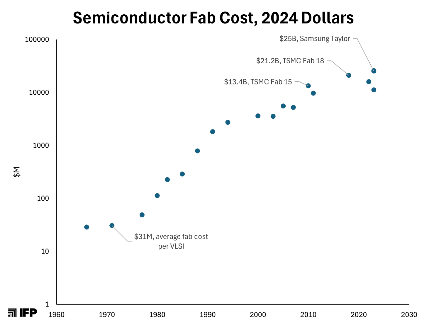
Just as Grove had feared in 2010, the pursuit of economic efficiency ultimately locked America’s chip companies “out of tomorrow’s emerging industry.” The continuous cycle of rapid adoption and technological improvements gave birth to Moore's Second Law, also known as Rock's Law (named after Arthur Rock, who first proposed this principle). The idea was that the cost of semiconductor fabs would double every four years. That has played out accurately, with the cost of a semiconductor fab rising from $31 million in the 1970s (adjusted to 2024 dollars) to at least $32 billion today; doubling in cost every five years.
The escalating costs of building semiconductor fabs have placed chip manufacturing beyond the financial reach of most fabless semiconductor companies. However, the consensus for years was that the lack of domestic chip manufacturing capacity wasn’t an issue. But the rate of acceleration in semiconductors, especially with AI, demonstrated more than ever that fabrication capabilities are far from a switch that can be turned on and off. The loss of capacity to produce leading-edge semiconductor nodes has created negative downstream effects, including a substantial lack of infrastructure in energy, machinery, specialized talent, and technical expertise.
For the majority of companies, that didn’t seem like a problem. But then in 2021, just about everyone realized it was a big problem.
The Return of Urgency
Chip shortages in 2021 impacted everyone. The auto industry’s inability to get adequate volumes of chips led to the production of 8 million fewer cars in 2021 than expected, resulting in $210 billion of lost revenue. Apple’s lack of access to chips forced the company to reduce iPhone production targets by 10 million units. Data center construction projects saw lead times increase by 52 weeks. Leaders across multiple industries began to recognize the critical vulnerability built within America's technology supply chain.
Concurrently, US military and government officials expressed increasing concern regarding America's technological dependence on a single foreign nation. Taiwan’s silicon shield had become a critical weakness for the US. If a Cold War II were to be fought between the US and China over a key resource bottleneck, it would be Taiwan that would represent the chokepoint.
China has repeatedly claimed sovereignty over the island of Taiwan, despite having never governed it. In October 2024, China asserted that Taiwan was a rogue province that would eventually be unified with the mainland by force. China increased its military presence near Taiwan by over 300% that same year.
Crucially, Taiwan represents a critical dependency for both consumer electronics and military capabilities. A large majority of US military systems require chips made from TSMC, such as the Lockheed F-35 fighter jet. With the increasing prevalence of AI in warfare, that dependence is only increasing. Shockingly, the US military is just as dependent on China for semiconductors as it is on Taiwan, with 40% of semiconductors for US weapons being built in China.
Meanwhile, unlike the US, China has been focused on onshoring and growing its domestic semiconductor production capability. As of 2024, China controlled 24% of the market for 50-180nm mature node semiconductors and, by 2030, is expected to represent 25% of the global supply for every type of semiconductor. China has prioritized capacity in advanced nodes with initiatives such as the National Integrated Circuit Industry Investment fund, which has invested over $150 billion to advance domestic production of advanced chips. Evidently, the CCP’s goal is chip sovereignty and has openly stated that the business of semiconductor manufacturing is the most important step for the development of China's "comprehensive national power."
Additionally, as China becomes more independent from Taiwan in terms of semiconductor manufacturing capacity, the risk of Chinese military intervention in Taiwan increases. Some preventative measures have been explored, such as threats from the US to “blow up TSMC” if China invades, and even Taiwan’s own efforts to install “remote self-destruct” capabilities in TSMC’s EUV machines.
While China’s stated ideological ends are reunification, its geopolitical aims may be more about cutting off the rest of the world from accessing TSMC’s chips and establishing a more dominant position in leading-edge semiconductor manufacturing. That could mean that gaining control over TSMC foundries isn’t even necessary, with one analyst questioning, “What if the reunification plan is based on eradicating the TSMC factories and the semiconductor supply chain in Taiwan and beyond?” If Taiwan and South Korea’s chip manufacturing capabilities were neutralized, China’s 12% of the global supply of semiconductors would quickly jump to ~33% of global capacity.
Without access to leading-edge chips, the West’s ability to maintain pace with cutting-edge AI will be severely limited. If we believe that the first nation to develop AGI will amass absolute power over its rivals, then it is rational for all nations to regard AI advancement as a national priority. In that regard, compute is the largest input to a nation’s push towards AI.
Accordingly, Anthropic’s CEO, Dario Amodei, argued in October 2024 that “if we want AI to favor democracy and individual rights, we are going to have to fight for that outcome.” Sam Altman, the CEO of OpenAI, said in July 2024 that “the urgent question of our time” is, “who will control the future of AI? Authoritarian governments the world over are willing to spend enormous amounts of money to catch up and ultimately overtake us.”
The AI race between China and the US in what has been dubbed Cold War II in some respects mirrors the Space Race between the US and the Soviet Union in the Cold War, in that both nations are competing over a critical technological capacity.
What differs is the stakes.
Whereas launching the first object into orbit or landing the first man on the moon were symbolic PR victories, AI will directly impact military strategies. What’s more, AI has an exponential trajectory; the better a nation’s AI capabilities get, the faster its AI technology will improve because it can use existing AI to help further accelerate its development of next-gen AI. This means there will be profound first-mover advantages that escalate over time for the nation that develops superior AI capabilities first, which is the opposite of what happens with most other military technologies – from gunpowder to nuclear weapons – which typically only confer a temporary window of advantage before those technologies proliferate to competitors.
If China were to invade Taiwan and destroy TSMC in a best-case scenario, or capture the company in a worst-case scenario, China would effectively neutralize global access to advanced semiconductors and secure a decisive advantage in AI development while expanding its domestic chip manufacturing capacity. What’s more, if a large-scale conflict were to escalate from Chinese intervention in Taiwan, the US military would be ill-equipped to compete with China, given its lack of access to this key battleground technology. The US’ supply of long-range anti-ship missiles would likely run out in around five days and could take years to replace.
America's vulnerability isn't hypothetical; it's urgent and unacceptable. We’ve woken up to the reality that dependence on TSMC and Taiwan creates a dangerous chokepoint, jeopardizing both our technological edge and national security. The question now isn't whether America needs its own TSMC. It’s how we get it.
An American Semiconductor Manufacturing Company: Build, Borrow, or Buy?
The simplest answer to the geopolitical conundrum created by our reliance on TSMC is that we need the willpower to build the American Semiconductor Manufacturing Company (ASMC) ourselves. But Rock’s Law makes this incredibly difficult. The cost of building a chip fabrication facility has steadily increased, growing from an estimated cost of $20 billion in 2020 to a staggering $45 billion foundry complex in 2025.
Source: Construction Physics
If the US wants to build ASMC, we have only a few options:
Option 1: Build ASMC from scratch
In theory, building ASMC from scratch simply requires a $20 billion check. The US government could, if prioritized, allocate this amount of capital to the effort. The check would cover:
Advanced manufacturing equipment: Each fabrication facility requires highly specialized machinery, like extreme ultraviolet (EUV) lithography machines, especially high-NA (numerical aperture) systems that can cost $380 million per unit. One fab would likely require 5 to 10 machines, a potentially multi-billion-dollar cost alone. That’s not even including the dozens of other necessary pieces of equipment required: chemical vapor deposition systems, sputtering machines, ion implanters, specialized chemicals, photoresists, and more.
Complex utility infrastructure: From stable power supply to water purification and waste management, a chip fab is like a city. Any limit to the fab’s control of its sophisticated environment could lead to significant inefficiency, so much so that some fabs have been “cancelled or relocated when local utilities can’t guarantee supply.”
Controlled cleanroom environments: Chip fabrication is such a precise art that it has to be conducted in ultra-clean environments that are thousands of times cleaner than a hospital operating room to avoid contamination. Those environments include advanced air filtration systems, temperature and humidity controls, and vibration-damping mechanisms, including deep concrete slabs designed specifically to eliminate even microscopic vibrations.
Overcoming regulatory hurdles: Under the National Environmental Policy Act (NEPA) and other stringent environmental protection laws, construction will take over 900 days (about 3 years) while costing four times more than equivalent facilities built overseas.
But that’s only to get the lights turned on. To effectively operate the fab will require expertise; expertise that America doesn’t have. Unfortunately, despite the US being the birthplace of the integrated circuit, the expertise to build leading-edge chips and manufacturing processes has largely relocated to Asia. Morris Chang’s key insight in the late 1960s and early 1970s was that learning curve theory would enable production costs to decrease as production volumes increased. But the advantage wasn’t just in cost reduction, it was in reps.
Fabricating leading-edge chips is one of the most complex manufacturing processes humanity has developed. It involves manipulating materials at the atomic scale, requiring thousands of separate process steps per wafer. That type of expertise doesn’t exist in the US, at least not much of it. When TSMC set out to build a plant in Arizona, the company had to send 600 American engineers to Taiwan for training.
The shortage of skilled workers in semiconductor manufacturing in the US is expected to reach 300K by 2030. Maybe, in the long run, the US can build out educational programs to increase that talent flow, but the reality of a highly specialized field like semiconductor manufacturing is that the education and practical experience go hand-in-hand. TSMC spends millions of dollars on university collaboration programs to fund research that supports part-time graduate degrees or on-site coursework. In addition, TSMC has built a “newcomer training center” that augments university studies with 3-6 months of ramp-time training, often continuing from TSMC-specific training in school as well.
Whereas Taiwan had decades to build these programs from scratch, the US is pressured not only by the limited number of students currently studying materials science that dominates the semiconductor industry, but by time, as China has aggressively poached semiconductor engineers at other firms. China has already blatantly recruited Taiwanese, Korean, and American semiconductor engineers and supports its workers with access to the latest research through hacking, forced technology transfers, and industrial espionage in what one former CIA senior intelligence officer has called “the greatest transfer of wealth in history.”
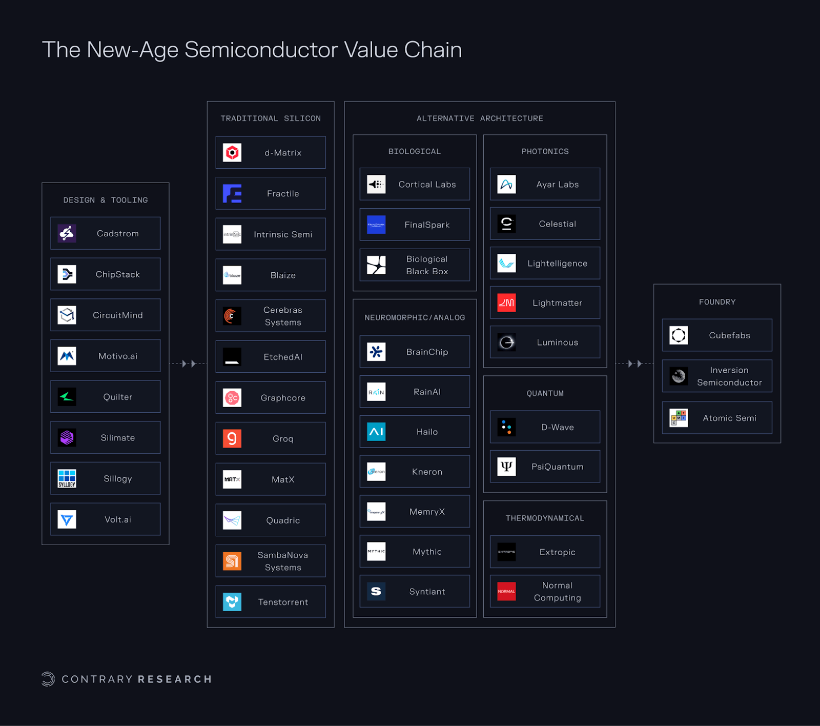
Building semiconductors domestically is a Herculean task, from the cost and complexity to developing talent. There are some companies making an attempt to rebuild American capability in semiconductors, from new chip design tools to new-age modular fabs, but these attempts will take too long to scale to reach meaningful production within the next 10 years. Below is an overview of many of the private companies that are innovating throughout the new-age semiconductor value chain.
Source: Contrary Research
The biggest obstacle for any company, whether they’re building a fab from scratch or building off of novel approaches, is achieving scale. Out of 1.2 trillion semiconductors sold globally, the US represents 25% of that demand, or roughly 300 billion chips. Granted, only a portion of those are leading-edge chips that TSMC provides. But regardless, the US is only manufacturing a fraction of the semiconductors it needs, and the looming conflict with China over Taiwan is not something that America has 10 or 20 years to plan for. It will likely occur in the near term.
As a result, building the American Semiconductor Manufacturing Company from scratch is not a viable option.
Option 2: Onshore TSMC to the US
Many view direct investment and partnership from TSMC in the US as our best chance. In 2021, TSMC broke ground on a 3.5 million-square-foot chip fab in Arizona. Originally expected to cost $16 billion, the facility ended up costing $20 billion. Its production focus was reportedly to be on producing 4nm chips at a volume of 20K chips per month. In December 2024, the company announced that its Arizona fab was expected to produce yield “right on par” with TSMC’s Taiwanese plants, though crucially at a higher cost per unit. By March 2025, the fab employed 3K people in Arizona. In addition, TSMC announced plans to invest $165 billion to build “three new fabrication plants, two advanced packaging facilities, and a major R&D team center,” resulting in the largest single foreign direct investment in US history.
However, TSMC’s Arizona foundry treats the symptoms, not the disease. First, even with all of TSMC’s efforts deployed in the US, TSMC’s two Arizona fabs are estimated to produce 600K wafers per year, compared to TSMC’s entire output of 16 million wafers (representing just 5-7% of TSMC’s capacity). Second, all of TSMC’s investments will be subject to regulatory review by Taiwan, and, increasingly, the company’s investments in the US are making the Taiwanese nervous. Critics of TSMC’s efforts in the US believe these efforts are an example of Taiwan’s ruling party “selling out Taiwan.”
Other potential attempts at further weaving TSMC into America’s semiconductor industry have been met with panic from many of the Taiwanese people who see America’s reliance on TSMC’s Taiwan factories as a feature, not a bug. First, in March 2025, there were rumors that TSMC had discussed acquiring Intel’s foundry business, which TSMC board member Paul Liu vehemently denied. Then, again in April 2025, there were rumors that Intel and TSMC had discussed a joint venture where TSMC would “operate Intel’s chipmaking facilities, with TSMC taking a 20% stake in the new company.” This time, TSMC refused to comment. However, the rumors “sparked an outcry in Taiwan about the chance of the country losing its silicon shield.”
Even if TSMC manages to get approval for the sizable investment it wants to make into the US, there are meaningful doubts about the long-term effectiveness of the effort. In April 2025, TSMC’s Chairman, C.C. Wei, indicated that the company may try to base “30% of future sub-2nm production in the US.” But the reality is that the majority of leading-edge research will always remain in Taiwan, allowing Taiwan to always monopolize the leading-edge chips that America desperately needs, strengthening Taiwan’s silicon shield.
In April 2025, Taiwan pushed forward a new law in response to semiconductor exports of expertise and IP. If implemented, the new law will “essentially [bar] TSMC from exporting its latest production nodes, and introduce penalties for violations.” This is another sign that, despite TSMC’s willingness to collaborate with the US, there is increasing pressure from the Taiwanese government to avoid doing so.
Beyond questions of where the leading-edge research would take place, some analysts indicate the effort to expand to America provides little business value to TSMC, where soaring construction costs for foundries and the cultural clashes between American and Taiwanese workers have directly impacted TSMC’s bottom line. American workers sent to Taiwan to train for a year complained about poor working conditions and inadequate training, while Taiwanese workers complained that Americans are arrogant and don’t have the work ethic for a semiconductor fab. One Taiwanese chemical supplier for TSMC saw costs at 10x what they were in Taiwan “due to the lack of production material supply and unfamiliarity with American regulations.”
Whether through internal pushback in Taiwan or external incompatibility with manufacturing builds in the US, our ability to rely on TSMC has more than enough obstacles to represent a stable, long-term semiconductor partnership.
Option 3: Buy the capability from Intel
If we can’t build the requisite capacity, and we can’t borrow it, could we buy it? But where do you buy a capable, leading-edge foundry business? In Santa Clara – the headquarters of Intel.
While the core trend lines of the American semiconductor industry have brought us to the current predicament, there is one company that has maintained consistency as an integrated device manufacturer (IDM): Intel. In fact, Intel is the only US-based company (out of three in the world) even attempting to manufacture leading-edge chips.
Two of Intel’s core businesses today are Intel Products and Intel Foundry. Intel Products has historically been the bulk of Intel’s business. This is the part of the business that designs new chips for PCs, laptops, servers, IoT, and more. Intel Foundry is the manufacturing part of Intel’s business. In the past, Intel focused exclusively on manufacturing its own chips. But increasingly, Intel is pushing for Intel Foundry to manufacture chips designed by other companies as well.
Intel’s foundry business already generates $17.5 billion in revenue, representing 33% of Intel’s total 2024 revenue, and has recently attracted customers like Microsoft, AWS, and Boeing.
Surprisingly, America’s foundry already exists!
But it’s struggling. While the foundry business represented 33% of revenue, it also generated a $13.4 billion loss, which represented 114% of Intel’s overall net loss for 2024. If we’re looking to buy our way into a rebuilt American semiconductor manufacturing industry, Intel is the only seller. The question is whether or not we’re willing to buy.
Rebuilding Intel as America’s Foundry
The centrality of Intel is the focus of the rest of this piece, because we believe it to be our best option to address the key national security risk posed by our lack of domestic semiconductor manufacturing capacity. That doesn't mean we shouldn’t try and get anything we can out of TSMC’s partnerships. That doesn’t mean startups shouldn’t pursue a new-age semiconductor value chain. But as Dylan Patel, a well-respected semiconductor analyst and founder of SemiAnalysis, has made clear:
“Intel Foundry’s survival is key to America’s national and economic security as the only domestic company with advanced logic R&D and manufacturing capability.”
That’s why, after a thorough exploration into the current semiconductor ecosystem, Intel rises to a place of prominence in our deep dive. The story of Intel illustrates how we broke our ability to build leading-edge chips, and what we have to do to build it back.
When Intel Ruled The World
While Intel has delivered poor results in the recent past, the company was once a dominant force contributing to US technological capability. In 1971, Intel released the Intel 4004, the first commercially available microprocessor in the world. In the earliest days of computing, Intel was a critical player; for example, the Intel 8080 was included in the Altair 8800 in 1974.
Intel spent decades consistently pushing forward semiconductor progress, especially during periods when Intel’s chips improved from 6000nm to 3000nm in the 1970s or from 45nm in 2007 to 22nm in 2011; a 51% reduction in just four years. By 2012, Intel’s Ivy Bridge processor not only pushed the industry to 22nm, but did it with an architecture that enabled 18% performance improvements at high voltage and 50% power reduction at constant performance. Over and over again, Intel was at the leading edge for decades:
2001: Intel was one of the first to develop a 64‑bit extension for its x86 architecture internally.
2003: Intel developed the Pentium M / Centrino to improve laptop-class efficiency.
2011: Intel became the first company (ahead of TSMC and Samsung) to ship mass‑produced 22nm CPUs using FinFET (3‑D “Tri‑Gate”) transistors, a breakthrough that reduced leakage current and improved performance‑per‑watt by moving from flat to three‑dimensional gates.
2016: Intel acquired Nervana Systems in an attempt to lead the charge on purpose-built AI silicon.
From 1972 to 2012, Intel stock increased 7,662% growing to more than $100 billion in market capitalization, up from $1.6 billion in 1985. But despite Intel’s reputation as a market leader, the cracks had already started to form in its ability to compete by the early 2000s. The failures would come from Intel’s inability to commercialize its own breakthroughs, a failure to bet on an increasingly critical piece of technology, and a transition from an engineering culture to a managerial culture. Eventually, after 25 years of being included as a key stock in the Dow Jones Industrial Average, Intel was removed from the index and replaced by Nvidia in November 2024. At its peak market cap in August 2000, Intel was valued at $509 billion, or $930 billion in 2024 dollars, making it the most valuable public company on Earth at the time. By May 2025, a quarter century later, it was valued 10x less at just $90 billion.
The Fall of Intel
One crucial impediment for Intel stemmed from its recurring inability to commercialize foundational investments.
2003: While Intel was one of the first to develop a 64-bit extension, AMD shipped it first with the AMD64.
2018: Despite Intel’s early success with FinFET transistors, TSMC and Samsung quickly overtook Intel with 10nm and 7nm processes.
2020: Just four years after Intel’s acquisition of Nervana Systems, Intel shut the group down, ceding AI-centric computing to Nvidia.
Beyond Intel’s seeming inability to get out of its own way, the company made a crucial mistake in one key area of breakthrough technology, despite once again being first on the scene. The technology? Extreme ultraviolet lithography (EUV).
An EUV machine is regarded as the standout equipment in any foundry process, used to pattern chip designs onto a silicon wafer. It is an incredibly sophisticated machine that is, effectively, shooting a laser at droplets of tin smaller than a dust particle to produce a specific wavelength of ultraviolet light. Each tin droplet is hit twice, once to flatten it and once to vaporize it, 50K times a second, generating a plasma that is 40x hotter than the surface of the sun. Founded in 1984, the Dutch company Advanced Semiconductor Materials Lithography (ASML) spent a decade figuring out how to build these kinds of machines, each of which can cost over $380 million.

Source: ASML
In 1997, Intel was among a group of companies alongside the US Department of Energy that created EUV LLC, a $250 million consortium to take EUV from theory to reality. In 1999, ASML joined the consortium. After years of working together to bring EUV into production, in 2012, Intel invested $3.1 billion into ASML for a 15% stake in the company and $1 billion in a joint venture around EUV. Once again, the stage was set for a leading-edge development in chip manufacturing, and Intel was at the forefront.
But when the time came to adopt EUV, rather than capitalizing on the investments Intel had made in EUV, it decided to stick with the outdated multi-pattern ArF lithography. Instead, it was TSMC that first adopted the technology and allowed it to surpass Intel to manufacture the 7nm node.
Source: WikiChip; Contrary Research
Without the new EUV lithography machine, Intel stumbled on its 10nm chip. In 2013, Intel established a production target for 2015, but this was repeatedly delayed due to low-quality early yields. In addition, Intel’s decision to stick with its older multi-pattern ArF lithography technology delayed its transition to the newer EUV lithography technology. By 2017, TSMC was mass-producing 10nm chips, while Intel was still releasing 14nm chips.
Source: WikiChip; Contrary Research
By 2018, TSMC began using EUV lithography for its 7nm chip. Intel wouldn’t achieve 7nm until 2021 and wouldn’t use EUV in production until the release of its 4nm chip in 2023, giving TSMC a five-year head start on deploying EUV technology throughout its processes. By the end of 2020, TSMC had 50% of all EUV installations globally. Since then, Intel has been playing catch-up to TSMC.
Source: WikiChip; Contrary Research
Despite Intel’s stumbles, there is still hope for its foundry division. While AMD’s spinout fab, GlobalFoundries, abandoned efforts to build leading-edge chips in 2018, Intel is targeting an ambitious production deadline for 2nm chips in late 2025, which would put it in line with TSMC’s 2nm rollout. Some industry analysts predict that Intel’s chips could be superior to TSMC's, while others are convinced that TSMC will maintain its lead. If Intel can successfully meet this deadline, it will be the fastest node advancement in semiconductor manufacturing history. This race is far from over.
But if Intel is going to not only hang onto the tentative grasp it has on the leading-edge, but pull ahead, it has to reckon with its own innovator’s dilemma.
The Innovator’s Dilemma For Intel
The needed reinvention of Intel is stymied by two core forces: (1) the emergence of a management culture over an engineering culture, and (2) an ongoing conflict of interest between chip fabrication and chip design that Intel has consistently ignored. Intel’s cracks had already been showing since at least 2015, when the company first delayed its 10nm chip, but only in the last few years has it become readily apparent that something has to change. Intel is staring down the barrel of the innovator’s dilemma, and it no longer has the option of doing nothing.
First, culture.
Intel’s status quo, in terms of culture, has been defined as driven by management as opposed to engineering. But Intel did not start out this way: its original founders, Robert Noyce, Gordon Moore, and Andy Grove, were considered generational engineers. The shift to managerial priorities began with the leadership of Paul Otellini, who was CEO of Intel from 2005 to 2013. He was the first Intel CEO who “was not formally trained in engineering.” In his first year, Otellini spent $10.6 billion in stock buybacks, and eventually would set a record in 2011 for spending $14.3 billion in stock buybacks, forgoing investment that could have gone into R&D. Instead, internal memos emphasized “efficiency” and “shareholder value” more than design excellence. In addition, Otellini put in motion the timeline for the 10nm chip, where Intel lost its lead.
From Otellini’s retirement in 2013 until 2021, Intel was run by managers. Otellini’s replacement, Brian Krzanich, accelerated the managerial bent by laying off 12K people while significantly increasing its efforts in hiring outside executives and raising his own salary by $3.5 million from the year before. Then, Bob Swan, who came from a pure finance background, continued to prioritize buybacks and margin preservation over any technical course correction. Over the course of several decades, Intel spent $152 billion on stock buybacks as opposed to investing in its own R&D. This figure, by the way, is roughly the amount TSMC planned to spend to build not only three new US foundries, but two additional advanced semiconductor packaging facilities in 2025 while accelerating R&D efforts.
It wasn’t until Pat Gelsinger took over in 2021 that any correction was put in place. Gelsinger focused his attention on undoing 15 years of financialization and, instead, made the effort to “bring back the geeks” and reestablish Intel’s engineering-first culture. Despite Gelsinger’s attempts, he was pushed out of the company in December 2024, likely because of the board’s lack of patience for his roadmap to reclaim Intel Foundry’s former glory. Still, his replacement, Lip-Bu Tan, is first and foremost an engineer, continuing Intel’s return to an engineering-first culture that Intel requires if it's going to reinvent itself.
The second part of Intel’s dilemma stems from a glaring conflict of interest.
Intel is one of the few companies that has maintained its status as an integrated device manufacturer, meaning it both designs and manufactures its own chips. In its continual race to keep pace with TSMC, Intel has had one meaningful disadvantage. TSMC is able to take advantage of Morris Chang’s learning curve theory and drive its progress through high volumes, producing 6-8 billion chips in 2024, as it can serve any number of customers. In contrast, Intel has been relatively limited to primarily manufacturing its own chips, producing just 600 million chips total in 2024, likely because only 2% of its capacity is reserved for external clients.
While Intel manufactures chips for Boeing or Microsoft, it has consistently refused to acknowledge the inherent risk it forces on fabless chip companies which could be potential customers. When Intel both designs and manufactures chips, it could easily steal sensitive IP from the designs of would-be customers to benefit Intel’s own chips.
Ironically, Intel should understand firsthand the risk here. In 1982, Intel signed a technology exchange contract with AMD to get additional capacity to produce its 8085 processor for IBM PCs. In 1987, after AMD used that arrangement to copy Intel’s processor microcode and compete directly with Intel, Intel had to sue AMD.
Any would-be Intel customers, like Nvidia, AMD, Qualcomm, Marvell, or Broadcom, would face the same risk in asking Intel to manufacture chips for them as long as Intel is also in the chip design business. For example, AMD has reportedly continued to say it has “no interest [in] working with Intel as its foundry.”
Similar conflicts of interest have caused breakups in other corners of the chip world. For years, Samsung was the sole manufacturer of Apple’s A-series chips, despite being Apple’s primary competitor in smartphones. Eventually, the competitive threat was too great and, in 2011, Apple sued Samsung for “slavishly copying” the iPhone. Speculatively, as a result, Apple started to dual-source its chips from Samsung and TSMC in 2015 before moving to TSMC exclusively in 2016.
If Intel is going to play the role of the American Semiconductor Manufacturing Company, it can’t maintain a business model that alienates the majority of customers who would represent significant demand for its foundry services. One obvious solution to this conflict is separating Intel’s foundry business from its chip design business.
In February 2025, four former Intel board members made that argument for the breakup of Intel. Their piece made the point that, on rumors of a potential Intel breakup, Intel’s stock surged 20%, so clearly they’re not the only ones excited by the prospect. The group of Intel board members argued that “[Intel] no longer generates enough profits from its design business to fund the enormously expensive, never-ending construction and reconstruction of its manufacturing plants to produce leading-edge chips.” Instead, the solution is to separate the manufacturing business:
“The right answer—and it’s been the right answer for years—is for the United States to insist that Intel split its twinned businesses. The United States government should demand that Intel’s board separate the manufacturing business, which can only be sold to a U.S. or Western consortium of private sector investors.”
In response, former Intel CEO Craig Barrett called this approach “the dumbest idea around.” Barrett, as the last engineering-led CEO before Otellini took over in 2005, instead focuses attention on Intel’s technical capabilities:
“Intel is back—from a technology point of view. They are still struggling to attract independent chip designers, but they have the technology and manufacturing know-how to compete with the likes of TSMC… The former board members think that because Intel also makes and sells chips, no other chip designers will want to trust Intel to make their products. This thought process ignores the fact that the best technology wins in the semiconductor industry.”
Pat Gelsinger, similarly, made it clear that he wouldn’t preside over the split of Intel’s businesses, saying, “if you want to split the company in two, then you should hire a PE kind of guy to go do that, not me.” Intel’s new CEO, Lip-Bu Tan, has said he would spin off assets that aren’t central, such as the sale of Altera, a company that makes field‑programmable gate arrays (FPGAs), of which Intel owned 51%, or spinning off RealSense, a computer vision subsidiary.
While Tan hasn’t explicitly advocated for selling Intel Foundry, he recently made it clear that it's far from safe from the chopping block. In July 2025, Tan announced that Intel Foundry is going to develop 18A for Intel Products, rather than external customers, and focus instead on developing 14A “based on confirmed customer commitments. There are no more blank checks. Every investment must make economic sense.” In the company’s Q2 2025 filing, it made the dire straits for Intel Foundry abundantly clear:
“We are focused on the continued development of Intel 14A… and on securing a significant external customer for such nodes. However, if we are unable to secure a significant external customer and meet important customer milestones for Intel 14A, we face the prospect that it will not be economical to develop and manufacture Intel 14A and successor leading-edge nodes on a go-forward basis. In such an event, we may pause or discontinue our pursuit of Intel 14A and successor nodes and various of our manufacturing expansion projects.”
As one analyst put it, this would be nothing short of the death of America’s Foundry. “That will lead to a massive write-down [on $100 billion worth of chip manufacturing equipment] as well as Intel becoming dependent on TSMC for chip manufacturing.” This cannot be allowed to happen. Intel Foundry needs to remain operational if the US wants any fighting chance of maintaining domestic leading-edge chip manufacturing.
What, then, should a revolutionized Intel look like?
Intel Reborn
In 2021, Pat Gelsinger laid out his vision for Intel: IDM 2.0. The focus was on expanding manufacturing operations with two new fabs in Arizona, reaching 7nm, launching new research collaborations with IBM, and getting reconnected to developers by bringing back the company’s developer forum event.
But the most critical aspect of IDM 2.0 was the creation of Intel Foundry Services.
Intel Foundry Services was launched with the explicit purpose of becoming a “major provider of foundry capacity” in the US and Europe. The unit was established as a standalone business unit with its own President, Dr. Randhir Thakur, who would report directly to Pat Gelsinger. Thakur had previously served as Intel’s Chief Supply Chain Officer. In addition, as a standalone business unit, Intel started to break out financial reporting for the Foundry business from an “Other” category in the company’s P&L starting in October 2022.
Unfortunately, Intel’s foray into independent foundry services has been rocky. Thakur, as President of Intel Foundry Services, only lasted two years. He was replaced by Stuart Pann, who, instead of President, was named senior vice president and general manager of Intel Foundry Services. He only lasted a year before Kevin O'Buckley from GlobalFoundries took over the same role in May 2024 for two months. After three different leaders in as many years, Intel decided in August 2024 to hire Naga Chandrasekaran as Chief Global Operations Officer, executive vice president, and general manager of Intel Foundry, which had rebranded from Intel Foundry Services in February 2024.
Right off the bat, Intel Foundry is plagued by leadership turnover. Despite ensuring that these leaders report directly to Intel’s CEO, the role also immediately diminished in control. The seniority of the role diminished from Thakur’s role as President to Chandrasekaran’s role as simply general manager.
In September 2024, Intel took an important step to break out Intel Foundry as an independent subsidiary that would offer “clearer separation and independence from the rest of Intel,” while also enabling greater “flexibility to evaluate independent sources of funding.” Intel Foundry would also have its own independent board of directors. But will it be enough?
If we’re going to buy into the vision of Intel Foundry becoming America’s Foundry, there are some things we believe we’ll have to see. And thus far, Intel’s half measures won’t be enough. It will require a more visionary leadership structure, a capital base built around growth over cost savings, and an emphasis on technical leadership over managerial order.
Buying Into ASMC: The Case For Intel
Building massively complex, highly scaled projects requires a completely different mindset from legacy platforms that are primarily good for harvesting consistent, or sometimes declining, earnings. Amazon building AWS or Netflix building a streaming service are fundamentally different from AT&T or IBM paying out 3-6% dividends with flat to negative revenue growth.
In 2006, Amazon was generating $10.5 billion in revenue selling books, clothes, and CDs online. But Jeff Bezos had a bigger idea. He wanted to rent out space on server racks stored in Amazon’s 10 million square feet of warehouses to run other people’s websites. Wall Street’s response was to “groan,” with a BusinessWeek headline reading “Wall Street wishes he would just mind the store.”

Source: MoneyControl
Fast forward to 2024, when AWS generated $107.6 billion in revenue; 6.5x more than the entire market cap of Amazon in November 2006. Taking massive bets requires key characteristics, from visionary leadership to a capital base built around growth over cost savings, and an emphasis on technical leadership over managerial order. For Amazon, AWS was a function of having cash to reinvest into building new business lines. That’s where Intel is at a disadvantage. Intel isn’t spitting off cash to reinvest in its reinvention as America’s Foundry. So what else can it do?
Case Study: Waymo
Another example of an ambitious big bet is Alphabet’s driverless car division, Waymo. Originally created in 2009 within Google’s moonshot factory, GoogleX, Waymo was later spun out as an independent company under the Alphabet umbrella in December 2016. At the time, Google had invested $1.1 billion in the project. Seeing the project as having grown beyond an R&D project, Alphabet spun it out for several key reasons:
Organization-Specific Leadership: Waymo was previously led by a project lead that reported to Google’s R&D structure, but became led first by CEO John Krafcik, then, in 2021, by co-CEOs, Tekedra Mawakana, the company’s prior COO and Head of Policy, and Dmitri Dolgov, one of the original leaders of Google’s driverless car project dating back to 2009, and then CTO of Waymo.
Independent Entity: Before, as a project within Google, Waymo’s equity structure was tied to Google’s overall business, but as a separate entity, Waymo is able to sign its own deals with partners, issue equity, and raise external capital.
Organization-Specific Equity: Prior to the spin-out, Waymo employees could only be incentivized with stock tied to Google’s overall performance. As an independent entity, Waymo’s employees can be incentivized with stock tied directly to Waymo’s success. Waymo’s employees can see its valuation grow to over $45 billion and understand their ownership of that specific asset.
Access to External Capital: As a business unit within Google, funding for Waymo’s development was primarily available only from Google’s operating cash flow. As an independent entity, Waymo has been able to 10x its access to capital, raising $11 billion in funding, both from strategic investors like AutoZone and Magna International, as well as financial investors like Silver Lake, T. Rowe Price, and a16z.
Intel has already taken some steps similar to aspects of Waymo’s journey towards independence, but there is a lot that Intel Foundry could benefit from in replicating this approach.
Visionary Leadership
First and foremost, the clear flaw in Intel’s approach to building Intel Foundry is its lack of commitment to a leader and a leadership structure. From Dr. Randhir Thakur being named President in March 2021, to a rapid cycle through four leaders in three years, to Naga Chandrasekaran being named, not president, but general manager, of Intel Foundry in August 2024. On top of that, he’s also serving as Intel’s Chief Global Operations Officer and Chief Technology Officer.
Contrast this with Waymo’s leadership approach. While the company has co-CEOs, each leader is clearly representative of a key requirement for Waymo to be successful. Driverless cars represent a new frontier of complex regulatory approvals and careful monitoring. Nobody wants a repeat of Cruise’s disastrous ban from San Francisco and ultimate failure. Tekedra Mawakana's career has been primarily in policy and regulatory management, including a stint as Waymo’s Head of Policy. She represents one-half of Waymo’s business. Dmitri Dolgov, as an original engineer on Google’s driverless car project back to 2009 and the former CTO of Waymo, is indicative of an engineering-first culture. Waymo is, at its core, solving a technology problem. The combination of Mawakana and Dolgov represents a recognition of Waymo’s fundamental levers.
Similarly, AWS was effectively co-founded by Andy Jassy within Amazon in 2003. Jassy became the CEO of AWS, led the operation through its launch in 2006 until 2021, when he replaced Jeff Bezos as the CEO of Amazon. Large, complex swings require leadership that is not only visionary in what they believe the operation can become and how it can get there, but also is structurally enabled to lead the effort, rather than be one of many voices driving the project’s direction.
Source: Intel News
Naga Chandrasekaran certainly has the background to be the leader that Intel Foundry needs. He spent over 20 years at Micron shipping frontier DRAM and NAND nodes on time, at scale, and with industry-leading density. He’s led teams across both R&D and manufacturing, and has continued to evaluate EUV performance for different processes. In addition, as an outsider, he’s less likely to fall victim to the potential bias of “Intel knows best” that a long-time Intel ‘lifer’ might be inclined to follow.
But Chandrasekaran’s role as Intel’s Chief Global Operations Officer and Chief Technology Officer is indicative of the way Intel views the foundry business today – as yet another piece of the Intel puzzle, not a fundamentally independent bet. Even as Intel attempts to further separate its businesses into Intel Foundry and Intel Products, the company has named Michelle Johnston Holthaus as the CEO of Intel Products. Why isn’t Naga Chandrasekaran the CEO of Intel Foundry?
Until Chandrasekaran, or someone else with the necessary capability, is able to lead Intel Foundry as a business with a vision to become America’s Foundry, just as Jassy led AWS to become the backbone of the internet, or Mawakana and Dolgov are driving Waymo to be the default autonomy transportation platform, Intel Foundry will fail to live up to its potential.
Even if Chandrasekaran is better positioned to be the leader of Intel Foundry than he needs to be, he’ll ultimately prove unsuccessful if it's simply his title that changes and not the system of incentives he’s able to build up around the business.
Growth Over Cost Efficiency
As investors and analysts discuss the potential value of Intel, they often describe the business in similar ways: compelling, but “shackled by the continuous drain of Intel’s foundry ambitions.” The focus on Intel’s value is on the design business because that has historically driven Intel’s revenue. As one report puts it, “once the foundry baggage is removed… Intel’s design group can stand on its own merits.” And, from the perspective of public market analysts, this may be true. The perspective of analyzing Intel as one company sees Intel Foundry as simply an uncomfortable “cost of a strategic reset.”
But what that perspective misses is both the financial opportunity and existential necessity of Intel Foundry’s success for the United States. As Raja Koduri writes:
“The ‘spreadsheet & powerpoint snakes’ – bureaucratic processes that dominate corporate decision-making – often fail to grasp the true cost of surrendering performance leadership. They optimize for minimizing quarterly losses while missing the bigger picture.”
Intel Foundry’s sights should be set on taking market share from TSMC when it comes to manufacturing third-party chips. Intel’s entire business of design, manufacture, and product sales combined generated $53 billion in 2024 revenue. Meanwhile, TSMC generated $90 billion in manufacturing revenue alone. That’s the size of the financial opportunity for Intel Foundry.
Meanwhile, China’s intentions with Taiwan could represent an existential threat to the US and a $10 trillion risk to the global economy. Intel Foundry is the only hope for America to rebuild semiconductor manufacturing capacity domestically quickly enough for a potential conflict with China, and in a way that isn’t tied to TSMC’s Taiwan operation. What a public analyst may see as a cost center for Intel is, in fact, an investment in America’s technological independence that can’t be justified through spreadsheets and formulas alone. Lip-Bu Tan may be demonstrating economic conservatism when he says “no more blank checks,” but at the same time, he’s signalling the fundamental misappropriation of resources when it comes to Intel Foundry.
What Intel Foundry needs is a capital structure that views it through the lens of a growth business, instead of a cost center for a chip design company. Investors need to understand the thesis behind Intel Foundry as a standalone business, driven by (1) becoming a “major provider of foundry capacity” in the US and Europe, (2) building a reputation as America’s Foundry in an increasingly deglobalized world, and (3) earning the support of the US government in pursuing that vision of becoming America’s Foundry.
Amazon’s AWS bet required a similar mentality. In fact, even outside of AWS, Amazon has consistently managed to turn cost centers into growth businesses. From logistics to technology to marketing to payment processing, Amazon has built businesses out of meaningful cost centers. Amazon invested over $20 billion into AWS before it became a profitable business in 2015.
Source: Amazon; Contrary Research
Similarly, TSMC has invested more than $300 billion over the course of the last 20 years to build a business that generates $90 billion of annual revenue and consistently produces 25-35% net income margins. In 2025 alone, TSMC plans to invest over $30 billion in additional capital expenditures. It turns out that building the most complicated device humans have ever made is expensive, but can be vastly rewarding if done well. Not just financially, but also in terms of preserving American technological independence.
Intel’s decision to start breaking out the Intel Foundry P&L in October 2022 was an important step in providing context on the business. But it isn’t a pretty picture. Declining revenue, worsening gross margins, and growing net losses. Intel Foundry’s losses contributed to the first overall profit loss for Intel since 1986. In addition, the financial picture led to multiple class action lawsuits against Intel executives, accusing them of misleading investors about the health of the business.
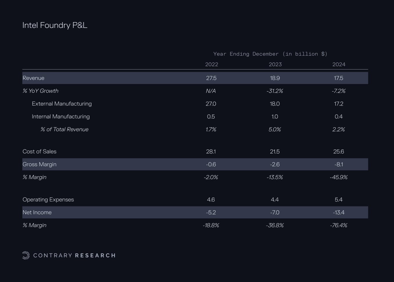
Source: Intel; Contrary Research
The biggest driver of Intel Foundry’s losses is its cost of sales, which includes accelerated depreciation on assets for building Intel 7 chips, and factory startup costs for Intel 3, 4, and 18A.
The clearest path to improving those margins? Yield. Yield refers to the percentage of chips on a wafer that function correctly and meet performance standards after fabrication. One key driver of yield is volume. If Intel Foundry can drive higher volumes of external customer demand, it can enable them to demonstrate quality.
Already, Intel is beginning to work with Boeing, Northrop Grumman, Microsoft, and IBM in some use cases, particularly around defense. But there is a clear benefit to working with hyperscalers across AWS, Google, Microsoft, Apple, Meta, and Nvidia more aggressively, all of which are incentivized to invest in semiconductor capacity independent of Taiwan, both in terms of geopolitical risk and domestic regulatory scrutiny. One approach for Intel Foundry could be structuring “take-or-pay” wafer pre-purchase contracts to get cash upfront while ensuring access to foundry capacity. One estimate indicated the volume each of these large tech customers may demand could represent $25 billion in pre-payments in the first year of such an agreement.
The US government can reinforce this thesis by investing in American silicon. In fact, the government has already started to support Intel’s efforts to become America’s Foundry by awarding the company $7.9 billion in funding as part of the CHIPS Act. In addition, Intel has won $3 billion as part of a secretive manufacturing program called the "Secure Enclave” with the Department of Defense.
But the government could do more than help fund Intel Foundry’s operation. First, it could ease regulatory pressure for large customers of Intel Foundry, whether through antitrust, privacy, or monopolistic practices. The influence of the US government could also ease regulatory pressure in Europe in exchange for offering them access to additional manufacturing capacity as well. Second, the US government could offer significant tax incentives to any large customers of Intel Foundry. This would demonstrate that committing to and investing in America’s Foundry would yield financial advantages.
This overarching thesis for Intel Foundry as an independent business, focused on taking market share from TSMC, garnering support from companies looking for domestic chip supply, and supported by the US government, could lead to an investor base for Intel Foundry aligned with its overall goal of growth versus cost-cutting. In fact, all of the potential customers above could take an equity stake in Intel Foundry, from the US government to the hyperscalers. In addition, financial investors who espouse an emphasis on American Dynamism, like a16z and Silver Lake, could also become financial investors.
The ability to focus on growth over cost efficiency may be possible as an independent subsidiary under the umbrella of Intel, similar to Waymo as part of Alphabet. But the significant investments and commensurate losses may be too much for the public markets to bear. It may make more sense for Intel Foundry to be rebuilt first as a private company with the capital support of the US government, customers, and capital partners. As Ben Thompson describes, “a standalone manufacturing business will have the most powerful incentive possible to make this transformation happen: the need to survive.”
In a hypothetical move, a consortium of enterprise and government stakeholders could take Intel Foundry private. As Intel sends up emergency flares, indicating that “it [may] not be economical to develop and manufacture…leading-edge nodes,” it is clear that the survival of Intel Foundry is a concern that will be settled now or never. The US government could support the effort and have a wholly domestic leading-edge chip manufacturer, vs. being at the mercy of Taiwan’s silicon shield. Intel Products would be free of what it sees as a cost center and could focus on other efforts, like CPUs. And domestic chip designers would have access to a much better fabrication partner: cheaper, because of government subsidies, and safer, because it would avoid international entanglements.
Regardless of whether Intel Foundry is publicly or privately traded, what these stakeholders are investing in isn’t just the hope of success in semiconductor capacity. The thesis behind Intel Foundry is a return to technical leadership, rather than simple managerial order.
Technical Leadership Over Managerial Order
There are two elements to Intel Foundry’s efforts to return to technical leadership: high-NA EUV and Intel Foundry’s 14A chips.
In a callback to Intel’s missed opportunity to be the first customer of extreme ultraviolet lithography (EUV) in the early 2010s, Intel has similarly been investing heavily in the next-generation high-NA EUV technology. This would unlock the ability to produce 2nm and 1.4nm logic nodes without double or triple patterning, essentially simplifying the production process. To lock in its lead in high-NA technology, Intel spent an estimated $2 billion in 2024 to secure all the available high-NA machines from ASML until 2025.
One key unlock of high-NA machines will be advancing plans for Intel Foundry’s 14A chips. Its 14A chips would cram 30% more transistors into the same space by pairing a new “gate-all-around” transistor design with a power network that feeds the chip from the back instead of through its crowded top layers (known as PowerVia Backside Power Delivery). With electricity traveling a shorter, cleaner path, each transistor can switch using less voltage, giving the chip up to 20% better performance per watt. That would represent the same speed as Intel’s 18A generation while using about one-third less power.
While the company’s 18A chips are entering risk production, which means the chip should be ready for volume production in late 2025, as of April 2025, Intel’s CEO announced that the company already has customers testing runs for 14A chips. In fact, while TSMC’s competing A14 chip is scheduled for production in 2028, Intel Foundry has the chance to leapfrog TSMC with its 14A chip scheduled for risk production in 2027. On top of that, because of Intel’s efforts to invest in high-NA lithography, TSMC’s chips will not have the advantage of leading-edge technology. TSMC may not even be able to invest in the technology until 2030, giving Intel Foundry a five-year head start.
But if, as Intel worries, the company is “unable to secure a significant external customer” for 14A, then all of this potential technical leadership will be for naught as Intel cedes its manufacturing operation and, with it, ushers in the death of domestic chip capability. Intel Foundry is dangling by a thread. America’s Foundry needs American support, from policymakers to domestic chip designers and chip consumers.
Who’s Buying?
The reality of America’s ability to rebuild its own semiconductor manufacturing capacity will depend on an investment in building the American Manufacturing Semiconductor Company. We can’t do it from scratch. We can’t borrow it from TSMC without obstacles. The only option is to buy into Intel Foundry.
Unfortunately, Intel Foundry is our only hope to decouple ourselves from Taiwanese risk at the caliber, speed, and volume necessary. With visionary leadership, an ability to invest in growth over cost efficiency, and an emphasis on technical leadership over managerial organization, Intel Foundry could have a real shot. With the right resources, Intel Foundry can become America’s Foundry. Because ultimately, that’s the end goal. Despite its storied past, Intel shouldn’t be saved just for the sake of saving Intel. It should be saved because it is a critical part of American national security and geopolitical strategic interests.
Rebuilding American Dominance
Even if Intel is able to endure a restructuring in such a way that it’s able to build Intel Foundry into America’s Foundry, it most certainly can’t do it alone. It needs an apparatus around it, from help with research to regulation, and retraining. In large part, this should be provided by the US government. Champions of free market capitalism may bristle at this kind of potential tipping of the scales, but the reality is that this is a requirement in an increasingly hopeless situation. And there are analogs for this kind of joint effort. For example, consider Rapidus in Japan.
Case Study: Rapidus
Rapidus is a Japanese semiconductor foundry established in August 2022 through investment from eight Japanese companies. In addition, the Japanese government earmarked $65 billion in subsidies for the industry through 2030. Rapidus was established with the goal of producing 2nm chips by 2027. Benefitting from the experience of allies, the Japanese Ministry of Economy, Trade and Industry in Japan also established the Leading-Edge Semiconductor Technology Center (LSTC) organization to research next-generation semiconductor technologies with the United States. This will assist Rapidus in establishing a design and manufacturing platform for next-generation semiconductors in Japan.
Construction on Rapidus’ factory in Chitose began in September 2023, supported by $2.5 billion from the Japanese government. In addition, ASML has pledged to open an office in Chitose to assist Rapidus. The Chitose foundry is expected to run pilot line tests in 2025, working both with Japanese clients and American companies like Tenstorrent.
The analog to Intel Foundry is clear. When a nation, like Japan, is intent on willing a capability into being, it can do so with a combination of public and private capital support, learning from the experience of allies, and emphasizing a specific technical milestone, like 2nm production. The US is in the exact same position, but with far loftier ambitions by necessity.
Building up some marginal capacity is not enough. Intel Foundry must leapfrog TSMC in technical capability and build towards capacity to support a large swath of the US demand for advanced semiconductors. No small feat. What’s more, the US must focus on investing in the broader semiconductor apparatus to ensure that we don’t fall behind. Intel Foundry may enable us to keep one hand on the future with high-NA lithography and 14A chips, but what about the next leading-edge node?
Nationalize Semiconductor Research
The semiconductor industry is built on the fundamentally exponential advancements that made Moore's Law prove true for so long. In 1954, each transistor in the four-transistor Regency TR-1 radio cost about $29.03 in 2024 dollars. A modern 9.89-billion-transistor AMD Ryzen 9 3900X costs $499, or roughly $0.00000005 per transistor. This means that the cost of a transistor has fallen by a factor of 600 million in 70 years. Over the past several decades, the cost and size of electronic computation have made possible every technological advancement that we take for granted today.
But that progress has disappeared.
Since the development of the 28nm node in 2011, transistor cost reductions promised by Moore’s Law have stagnated. In fact, transistor costs have actually increased, rising to $1.52 per 100 million transistors for the 7nm nodes manufactured at TSMC today. This matches the same cost seen around 2005 for the 28nm node transistor.
While geometric scaling continues to pack more transistors per unit area (current 5nm nodes achieve roughly 120 times higher transistor density than the 90nm node) through pitch reduction and architectural innovations, this advantage no longer yields net cost reductions per transistor. The manufacturing complexity of these nanoscopic, and soon, angstromic, transistors requires extreme capital intensity and process complexity.
From EUV machines costing $350 million each to novel three-dimensional transistor structures that require atomic precision, total wafer costs have exploded from roughly $2.9K at the 28nm economic optimum to a rumored $45K for TSMC’s latest 1.6nm node. Unfortunately, exponential cost scaling has outpaced logarithmic density improvements. Moore’s law, at least in the economic sense, has already died. The pursuit remains now in technological progress, which is slowing down as well.
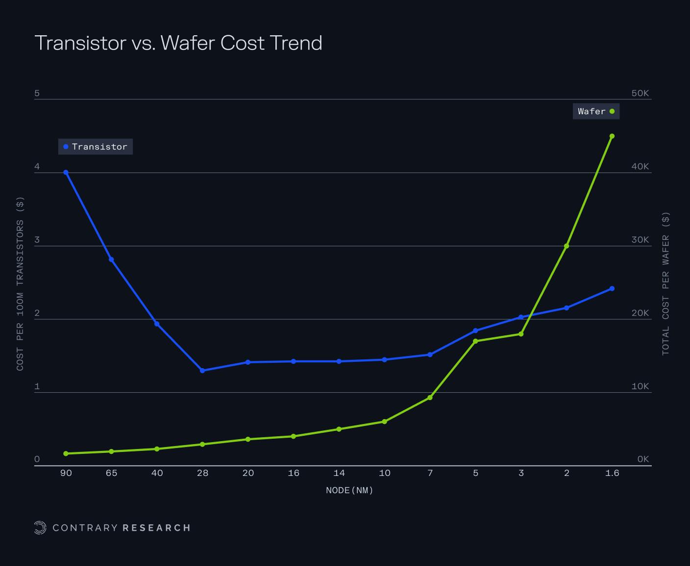
Source: AnySilicon; Contrary Research
Reestablishing that progress needs to become a national priority.
But innovating at the transistor level may be a dead end. Chip performance is now increasingly constrained by the physical limits of transistor size. Some predict that, by 2035, the smallest feasible silicon transistor will have been developed. While we can continue packing more transistors into each chip, individual transistor speed improvements have stalled. Dennard scaling is a principle that originally stated that as transistors shrink, voltage and current scale down proportionally, keeping the power density used by a chip constant even as more transistors are used. However, since 2006, Dennard scaling has broken down, leading to increased power usage of chips. Thus, modern-day chips are said to have hit a “power wall,” limiting further gains from transistor miniaturization.
The lowest-hanging fruit for continued innovation may be identifying a new paradigm shift in semiconductor architecture or computing more broadly.
One option could be new semiconductor materials. Just as TI led the transition from germanium to silicon transistors, or IBM’s use of copper over aluminum interconnects, there is potential for new material unlocks. In December 2022, Intel announced progress on new materials, “just 3 atoms thick,” that could lead to 10x improvements in transistor density by 2030.
Another could be specialized chips optimized for specialized workloads. It’s unlikely that, as chips become increasingly optimized, the best performance for a given application will come from a general-purpose chip. Unique use cases could benefit from customized architecture. One example is Nvidia’s Blackwell B200, which was purpose-built for AI use cases. The chip was announced in March 2024 and promised a 30x improvement compared to Nvidia’s general-purpose chips. This was followed up by Nvidia’s Blackwell Ultra GB300 in March 2025: Nvidia’s AI “superchip.”
Finally, another approach could be to fundamentally replace the transistor as the atomic computing unit. For the past 80 years of the computing industry, engineers focused on the transistor because it was the first scalable and mass-commercialized atomic computing unit after vacuum tubes. This has led to a homogeneous compute architecture. Alternative models could be photonic computing by companies like Lightmatter, thermodynamic computing by companies like Normal Computing, or biological computing by companies like Cortical Labs; any of which could potentially be faster and scale better, even if these technologies are still nascent.
While it’s unclear which approach could unlock future advances, it is clear that the semiconductor industry needs to unlock them. A large part of the research into new semiconductor materials, specialized chips, or alternative computing models could be supported by the government. The presence of federal support for this work could entice a commensurate volume of private capital investments as well, which could further spur the industry.
Government support for semiconductor manufacturing has already been demonstrated through large programs like the CHIPS Act. Announced in August 2022, this $53 billion program intends to boost domestic research and manufacturing of semiconductors in the US. By March 2024, some estimates indicated the program had incentivized around $175 billion of private capital into new projects. However, bureaucratic hurdles have delayed the deployment of tens of billions in funding.
While President Trump has expressed dissatisfaction with the CHIPS Act, which could threaten its longevity, he has also touted significant investments in the US semiconductor industry, such as TSMC’s $165 billion and Nvidia’s supposed $500 billion for “AI superchips.”
However, the government’s role doesn’t need to be exclusively as a funding mechanism. There is also a role to play in removing the barriers in the industry.
Deregulate Semiconductor Manufacturing
One critical regulatory obstacle for semiconductor manufacturing is the National Environmental Policy Act (NEPA). It was passed in 1969, which required federal agencies to produce a detailed statement of environmental impacts for any action that “significantly” affects the environment. Although it was passed with good intentions to protect the environment, it has now become the hallmark of stagnation in the US.
NEPA is directly responsible for slowing progress in US infrastructure, with economic growth slowing down in the early 1970s, right as NEPA was implemented. Different interest groups wield NEPA like weapons to blockade crucial US infrastructure projects. In practice, the citizen input function of NEPA has been used not to enact environmental justice but to let wealthy communities oppose projects — including transportation and public works projects — that inconvenience them. Moreover, litigation under NEPA is almost always local, meaning that a project’s regional or even national benefits are often devalued or disregarded.
As a result, innovation is inhibited by both labor resistance and a bureaucracy that has neither the incentives nor the capability of driving change. Accordingly, construction productivity has fallen by half since the 1960s.
NEPA can also be applied to federally funded semiconductor manufacturing projects, such as the CHIPS Act and TSMC’s Arizona foundry. Thus, semiconductor foundry projects must provide environmental assessments, and if the impact is deemed sufficiently severe, the agency must draft an environmental impact statement, taking an average of 4.5 years. This NEPA-based NIMBYISM is the main reason why semiconductor fabs are difficult to build in the US.
We need to follow Germany’s example in allowing exceptions for the semiconductor industry to build fabs, treating it as a matter of national security. Facing the urgent need to replace Russian gas, Germany enacted legislation that would bypass European Union procedural requirements — including its environmental impact assessment framework analogous to NEPA — specifically to expedite liquefied natural gas (LNG) infrastructure development.
In fact, Intel has already demonstrated that flexible permitting can work with its foundry in Oregon. Rather than getting a new permit every time the company wanted to tweak its manufacturing process, Intel got a flexible permit that set overall emission caps and pre-approved production changes for the Oregon facility. Intel proved that flexible permitting could deliver not only better environmental outcomes, but also operational flexibility, and continued domestic investment. This needs to happen again.
The Trump administration has recognized this issue, estimating that NEPA and other related laws could cost the US economy $3.7 trillion in lost GDP. Modernizing NEPA will both better ensure it isn’t abused and make sure that it becomes an unlock for semiconductor manufacturing to thrive. But marginal easing of regulatory pressure would likely be inadequate. Unlocking the semiconductor industry will need drastic action.
With research being subsidized and manufacturing capacity unlocked, the last critical question is whether or not we have an adequate labor force to put this engine into motion.
The Next Generation of Semiconductor Engineers
While many of the bottlenecks in semiconductor manufacturing feel like they’re at a boiling point – from geopolitical risk in Taiwan to American reshoring of manufacturing capacity – there is one critical bottleneck that is killing us slowly, and will take years to rectify: labor shortages.
Creating a single leading-edge chip involves hundreds of full-time engineers working for months, and that’s just for the design phase. There may be some alleviation to this issue, like leveraging generative AI to shrink the per-unit labor costs of chip design. Much of chip design is writing code that represents logic on a semiconductor and then writing verification scripts to test that logic. Several companies, such as Volt.ai, Cadstrom, Silimate, Sillogy, Motivo.ai, Quilter, Chipstack.ai, and CircuitMind, are attempting to incorporate AI into the chip design process.
However, chip designs and codes used to generate and verify them are closely guarded secrets, leaving a hefty gap in available training data.
Despite potential lifts from generative AI in some aspects of the chip creation process, the reality is that the US needs to invest in additional labor pools for semiconductor manufacturing. This could represent a shift from traditional blue-collar jobs to "silicon workers." We also need more community college programs, university partnerships, and direct industry training, mirroring TSMC’s efforts in Taiwan.
Taiwan’s chip sector has built a deep, purpose-trained labor pool despite its smaller population. One 2023 estimate put the island’s integrated-circuit workforce at about 120K people; roughly one skilled semiconductor worker for every 190 citizens, versus one for every 960 Americans in the US. TSMC alone employed 83K engineers and technicians in 2024 and runs an eight-week in-house academy that every new engineer must complete before entering a fab. Close coordination between the government and nine universities has also created dedicated semiconductor colleges and R&D institutes that channel graduates straight into fabs and equipment makers.
In the US, we could have a shortage of 300K unfilled semiconductor roles by 2030. Half of US master’s-level engineering graduates and 60% of PhDs are foreign nationals, and immigration rules send roughly 16K advanced-degree engineers abroad each year. Decades of offshoring have eroded “learning on the line” experience with new fabs in Arizona, Ohio, and upstate New York, having already had to import Taiwanese trainers because local technicians lacked hands-on EUV or high-vacuum tool skills.
Closing the gap will take a mix of domestic training and smarter immigration. Community college apprenticeships could be set up near fabs, funding technician “boot camps,” and attracting more STEM students into chip careers. In addition, the CHIPS Act’s workforce fund and upcoming National Semiconductor Technology Center could give those types of programs a federal spine. Finally, the US could fast-track green cards for advanced STEM graduates who could immediately plug the highest-skill holes.
Building the American Semiconductor Manufacturing Company
The history of the semiconductor is the history of the United States. From inventor, to manufacturer, to consumer, to hostage. The US has had a complex relationship with the atomic unit of computing, as it has become the single building block upon which American technological independence will live or die. The only response to our current situation is to build the American Semiconductor Manufacturing Company.
But we cannot beg, borrow, or build our way to ASMC with ease. Intel is our only hope as a flagship leader in the return to American semiconductor manufacturing capacity. However, despite Intel’s central role in this thesis, Intel is ultimately not the American Semiconductor Manufacturing Company. ASMC is an ideal; an ecosystem.
From the support of the US government in funding and incentivizing a loyalty to domestic semiconductor manufacturing, to a loyal base of American technology companies willing to commit to American semiconductor capacity, to Intel Foundry leading the charge in building back American capability, to new-age startups building new chip designs, investigating semiconductor materials, and new computing paradigms.
Together, that ecosystem can take America from a semiconductor consumer to a semiconductor creator.
If we fail, we may maintain exceptional chip design leadership, but we’ll continue to be held hostage to a flashpoint in the Taiwan Strait. If we succeed, America regains sovereign control over the computational substrate on which economic growth, military deterrence, and democratic AI all depend.
The question now is whether we are up to the task.